
Data Sheet

85
ATmega48A/PA/88A/PA/168A/PA/328/P [DATASHEET]
Atmel-8271H-AVR- ATmega-Datasheet_08/2014
• ICP1/CLKO/PCINT0 – Port B, Bit 0
ICP1, Input Capture Pin: The PB0 pin can act as an Input Capture Pin for Timer/Counter1.
CLKO, Divided System Clock: The divided system clock can be output on the PB0 pin. The divided system clock
will be output if the CKOUT Fuse is programmed, regardless of the PORTB0 and DDB0 settings. It will also be
output during reset.
PCINT0: Pin Change Interrupt source 0. The PB0 pin can serve as an external interrupt source.
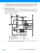
Table 14-4 and Table 14-5 on page 86 relate the alternate functions of Port B to the overriding signals shown in
Figure 14-5 on page 81. SPI MSTR INPUT and SPI SLAVE OUTPUT constitute the MISO signal, while MOSI is
divided into SPI MSTR OUTPUT and SPI SLAVE INPUT.
Notes: 1. INTRC means that one of the internal RC Oscillators are selected (by the CKSEL fuses), EXTCK means that
external clock is selected (by the CKSEL fuses)
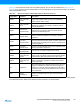
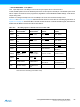
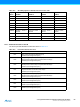
Table 14-4. Overriding Signals for Alternate Functions in PB7...PB4
Signal
Name
PB7/XTAL2/
TOSC2/PCINT7
(1)
PB6/XTAL1/
TOSC1/PCINT6
(1)
PB5/SCK/
PCINT5
PB4/MISO/
PCINT4
PUOE
INTRC
• EXTCK+
AS2
INTRC
+ AS2 SPE • MSTR SPE • MSTR
PUOV 0 0 PORTB5 • PUD PORTB4 • PUD
DDOE
INTRC
• EXTCK+
AS2
INTRC
+ AS2 SPE • MSTR SPE • MSTR
DDOV0000
PVOE 0 0 SPE • MSTR SPE • MSTR
PVOV 0 0 SCK OUTPUT
SPI SLAVE
OUTPUT
DIEOE
INTRC
• EXTCK +
AS2 + PCINT7 •
PCIE0
INTRC
+ AS2 +
PCINT6 • PCIE0
PCINT5 • PCIE0 PCINT4 • PCIE0
DIEOV
(INTRC + EXTCK) •
AS2
INTRC • AS2 11
DI PCINT7 INPUT PCINT6 INPUT
PCINT5 INPUT
SCK INPUT
PCINT4 INPUT
SPI MSTR INPUT
AIO Oscillator Output
Oscillator/Clock
Input
––