
Data Sheet

319
ATmega48A/PA/88A/PA/168A/PA/328/P [DATASHEET]
Atmel-8271H-AVR- ATmega-Datasheet_08/2014
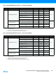
Notes: 1. “Max” means the highest value where the pin is guaranteed to be read as low
2. “Min.” means the lowest value where the pin is guaranteed to be read as high
3. Although each I/O port can sink more than the test conditions (20mA at V
CC
= 5V, 10mA at V
CC
= 3V) under steady state conditions (non-transient), the
following must be observed:
ATmega168P:
1] The sum of all I
OL
, for ports C0 - C5, ADC7, ADC6 should not exceed 100mA
2] The sum of all I
OL
, for ports B0 - B5, D5 - D7, XTAL1, XTAL2 should not exceed 100mA
3] The sum of all I
OL
, for ports D0 - D4, RESET should not exceed 100mA
If I
OL
exceeds the test condition, V
OL
may exceed the related specification. Pins are not guaranteed to sink current greater than the listed test condition
4. Although each I/O port can source more than the test conditions (20mA at V
CC
= 5V, 10mA at V
CC
= 3V) under steady state conditions (non-transient), the
following must be observed:
ATmega168P:
1] The sum of all I
OH
, for ports C0 - C5, D0- D4, ADC7, RESET should not exceed 150mA
2] The sum of all I
OH
, for ports B0 - B5, D5 - D7, ADC6, XTAL1, XTAL2 should not exceed 150mA
If II
OH
exceeds the test condition, V
OH
may exceed the related specification. Pins are not guaranteed to source current greater than the listed test condition
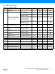
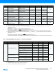
30.2.1 ATmega48PA DC Characteristics – Current Consumption
Notes: 1. Results obtained using external clock and methods described in ”Minimizing Power Consumption” on page 43. Power reduction fully enabled (PRR = 0xFF)
and with no I/O drive.
2. Typical values at 25°C. Maximum values are test limits in production
3. The current consumption values include input leakage current
I
IL
Input Leakage
Current I/O Pin
V
CC
= 5.5V, pin low
(absolute value)
1
µA
I
IH
Input Leakage
Current I/O Pin
V
CC
= 5.5V, pin high
(absolute value)
1
R
RST
Reset Pull-up Resistor 30 60
k
R
PU
I/O Pin Pull-up Resistor 20 50
V
ACIO
Analog Comparator
Input Offset Voltage
V
CC
= 5V
V
in
= V
CC
/2
<10 40 mV
I
ACLK
Analog Comparator
Input Leakage Current
V
CC
= 5V
V
in
= V
CC
/2
-50 50 nA
t
ACID
Analog Comparator
Propagation Delay
V
CC
= 2.7V
V
CC
= 4.0V
750
500
ns
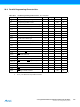
Symbol Parameter Condition Min. Typ.
(2)
Max. Units
I
CC
Power Supply Current
(1)
Active 1MHz, V
CC
= 2V 0.22 0.55
mA
Active 4MHz, V
CC
= 3V 1.15 2.65
Active 8MHz, V
CC
= 5V 4.1 9.5
Idle 1MHz, V
CC
= 2V 0.024 0.16
Idle 4MHz, V
CC
= 3V 0.2 0.75
Idle 8MHz, V
CC
= 5V 0.78 2.8
Power-save mode
(3)
32kHz TOSC enabled, V
CC
=1.8V
µA
32kHz TOSC enabled, V
CC
= 3V
Power-down mode
(3)
WDT enabled, V
CC
= 3V 3.9 8.5
WDT disabled, V
CC
= 3V 0.1 3
Symbol Parameter Condition Min. Typ. Max. Units