
Data Sheet

300
ATmega48A/PA/88A/PA/168A/PA/328/P [DATASHEET]
Atmel-8271H-AVR- ATmega-Datasheet_08/2014
29. Electrical Characteristics – (T
A
= -40°C to 85°C)
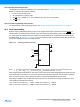
29.1 Absolute Maximum Ratings*
29.2 DC Characteristics
Operating Temperature . . . . . . . . . . . -55C to +125C
*NOTICE: Stresses beyond those listed under “Absolute
Maximum Ratings” may cause permanent dam-
age to the device. This is a stress rating only and
functional operation of the device at these or
other conditions beyond those indicated in the
operational sections of this specification is not
implied. Exposure to absolute maximum rating
conditions for extended periods may affect
device reliability.
Storage Temperature. . . . . . . . . . . . . -65°C to +150°C
Voltage on any Pin except RESET
with respect to Ground . . . . . . . . . .-0.5V to V
CC
+0.5V
Voltage on RESET
with respect to Ground-0.5V to +13.0V
Maximum Operating Voltage . . . . . . . . . . . . . . . . .6.0V
DC Current per I/O Pin . . . . . . . . . . . . . . . . . . 40.0mA
DC Current
V
CC
and GND Pins. . . . . . . . . . . 200.0mA
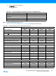
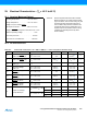
Table 29-1. Common DC characteristics T
A
= -40C to 105C, V
CC
= 1.8V to 5.5V (unless otherwise noted)
Symbol Parameter Condition Min. Typ. Max. Units
V
IL
Input Low Voltage, except
XTAL1 and RESET pin
V
CC
= 1.8V - 2.4V
V
CC
= 2.4V - 5.5V
-0.5
-0.5
0.2V
CC
(1)
0.3V
CC
(1)
V
V
IH
Input High Voltage, except
XTAL1 and RESET pins
V
CC
= 1.8V - 2.4V
V
CC
= 2.4V - 5.5V
0.7V
CC
(2)
0.6V
CC
(2)
V
CC
+ 0.5
V
CC
+ 0.5
V
V
IL1
Input Low Voltage,
XTAL1 pin
V
CC
= 1.8V - 5.5V -0.5 0.1V
CC
(1)
V
V
IH1
Input High Voltage,
XTAL1 pin
V
CC
= 1.8V - 2.4V
V
CC
= 2.4V - 5.5V
0.8V
CC
(2)
0.7V
CC
(2)
V
CC
+ 0.5
V
CC
+ 0.5
V
V
IL2
Input Low Voltage,
RESET pin
V
CC
= 1.8V - 5.5V -0.5 0.1V
CC
(1)
V
V
IH2
Input High Voltage,
RESET
pin
V
CC
= 1.8V - 5.5V 0.9V
CC
(2)
V
CC
+ 0.5 V
V
IL3
Input Low Voltage,
RESET pin as I/O
V
CC
= 1.8V - 2.4V
V
CC
= 2.4V - 5.5V
-0.5
-0.5
0.2V
CC
(1)
0.3V
CC
(1)
V
V
IH3
Input High Voltage,
RESET pin as I/O
V
CC
= 1.8V - 2.4V
V
CC
= 2.4V - 5.5V
0.7V
CC
(2)
0.6V
CC
(2)
V
CC
+ 0.5
V
CC
+ 0.5
V
V
OL
Output Low Voltage
(4)
except RESET pin
I
OL
= 20mA, V
CC
= 5V
T
A
=85C0.9
T
A
=105C1.0
I
OL
= 10mA, V
CC
= 3V
T
A
=85C0.6
T
A
=105C0.7V