
Data Sheet

297
ATmega48A/PA/88A/PA/168A/PA/328/P [DATASHEET]
Atmel-8271H-AVR- ATmega-Datasheet_08/2014
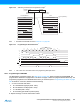
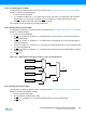
8. Power-off sequence (if needed):
Set RESET
to “1”.
Turn V
CC
power off.
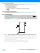
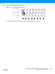
28.8.3 Serial Programming Instruction set
Table 28-19 on page 297 and Figure 28-8 on page 298 describes the Instruction set.
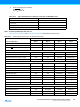
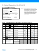
Table 28-18. Typical Wait Delay Before Writing the Next Flash or EEPROM Location
Symbol Minimum Wait Delay
t
WD_FLASH
4.5ms
t
WD_EEPROM
3.6ms
t
WD_ERASE
9.0ms
t
WD_FUSE
4.5ms
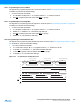
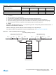
Table 28-19. Serial Programming Instruction Set (Hexadecimal values)
Instruction/Operation
Instruction Format
Byte 1 Byte 2 Byte 3 Byte4
Programming Enable $AC $53 $00 $00
Chip Erase (Program Memory/EEPROM) $AC $80 $00 $00
Poll RDY/BSY $F0 $00 $00 data byte out
Load Instructions
Load Extended Address byte
(1)
$4D $00 Extended adr $00
Load Program Memory Page, High byte $48 $00 adr LSB high data byte in
Load Program Memory Page, Low byte $40 $00 adr LSB low data byte in
Load EEPROM Memory Page (page access) $C1 $00 0000 000aa data byte in
Read Instructions
Read Program Memory, High byte $28 adr MSB adr LSB high data byte out
Read Program Memory, Low byte $20 adr MSB adr LSB low data byte out
Read EEPROM Memory $A0 0000 00aa aaaa aaaa data byte out
Read Lock bits $58 $00 $00 data byte out
Read Signature Byte $30 $00 0000 000aa data byte out
Read Fuse bits $50 $00 $00 data byte out
Read Fuse High bits $58 $08 $00 data byte out
Read Extended Fuse Bits $50 $08 $00 data byte out
Read Calibration Byte $38 $00 $00 data byte out
Write Instructions
(6)
Write Program Memory Page $4C adr MSB
(8)
adr LSB
(8)
$00
Write EEPROM Memory $C0 0000 00aa aaaa aaaa data byte in
Write EEPROM Memory Page (page access) $C2 0000 00aa aaaa aa00 $00
Write Lock bits $AC $E0 $00 data byte in