
Data Sheet

291
ATmega48A/PA/88A/PA/168A/PA/328/P [DATASHEET]
Atmel-8271H-AVR- ATmega-Datasheet_08/2014
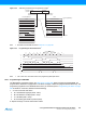
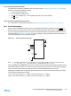
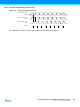
Figure 28-2. Addressing the Flash Which is Organized in Pages
(1)
Note: 1. PCPAGE and PCWORD are listed in Table 28-11 on page 286.
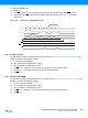
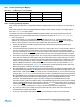
Figure 28-3. Programming the Flash Waveforms
(1)
Note: 1. “XX” is don’t care. The letters refer to the programming description above.
28.7.5 Programming the EEPROM
The EEPROM is organized in pages, see Table 28-12 on page 286. When programming the EEPROM, the
program data is latched into a page buffer. This allows one page of data to be programmed simultaneously. The
programming algorithm for the EEPROM data memory is as follows (refer to ”Programming the Flash” on page
289 for details on Command, Address and Data loading):
1. A: Load Command “0001 0001”.
2. G: Load Address High Byte (0x00 - 0xFF).
3. B: Load Address Low Byte (0x00 - 0xFF).
4. C: Load Data (0x00 - 0xFF).
5. E: Latch data (give PAGEL a positive pulse).
K: Repeat 3 through 5 until the entire buffer is filled.
PROGRAM MEMORY
WORD ADDRESS
WITHIN A PAGE
PAGE ADDRESS
WITHIN THE FLASH
INSTRUCTION WORD
PAGE
PCWORD[PAGEMSB:0]:
00
01
02
PAGEEND
PAGE
PCWORDPCPAGE
PCMSB
PAGEMSB
PROGRAM
COUNTER
RDY/BSY
WR
OE
RESET +12V
PAGEL
BS2
0x10 ADDR. LOW
ADDR. HIGH
DATA
DATA LOW DATA HIGH
ADDR. LOW DATA LOW DATA HIGH
XA1
XA0
BS1
XTAL1
XX XX
XX
ABCDEBCDEGH
F