
Data Sheet


287
ATmega48A/PA/88A/PA/168A/PA/328/P [DATASHEET]
Atmel-8271H-AVR- ATmega-Datasheet_08/2014
The XA1/XA0 pins determine the action executed when the XTAL1 pin is given a positive pulse. The bit coding
is shown in Table 28-15.
When pulsing WR
or OE, the command loaded determines the action executed. The different Commands are
shown in Table 28-16.
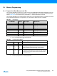
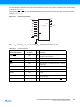
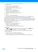
Figure 28-1. Parallel Programming
Note: V
CC
- 0.3V < AV
CC
< V
CC
+ 0.3V, however, AV
CC
should always be within 4.5 - 5.5V
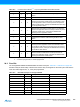
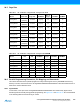
Table 28-13. Pin Name Mapping
Signal Name in
Programming Mode Pin Name I/O Function
RDY/BSY PD1 O
0: Device is busy programming, 1: Device is
ready for new command
OE
PD2 I Output Enable (Active low)
WR
PD3 I Write Pulse (Active low)
BS1 PD4 I
Byte Select 1 (“0” selects Low byte, “1” selects
High byte)
XA0 PD5 I XTAL Action Bit 0
XA1 PD6 I XTAL Action Bit 1
PAGEL PD7 I
Program memory and EEPROM Data Page
Load
BS2 PC2 I
Byte Select 2 (“0” selects Low byte, “1” selects
2’nd High byte)
DATA {PC[1:0]: PB[5:0]} I/O Bi-directional Data bus (Output when OE is low)
VCC
GND
XTAL1
PD1
PD2
PD3
PD4
PD5
PD6
PC[1:0]:PB[5:0]
DATA
RESET
PD7
+12 V
BS1
XA0
XA1
OE
RDY/BSY
PAGEL
PC2
WR
BS2
AVCC
+4.5 - 5.5V
+4.5 - 5.5V