
Data Sheet


280
ATmega48A/PA/88A/PA/168A/PA/328/P [DATASHEET]
Atmel-8271H-AVR- ATmega-Datasheet_08/2014
Write, or if no SPM instruction is executed within four clock cycles. The CPU is halted during the entire Page
Write operation if the NRWW section is addressed.
• Bit 1 – PGERS: Page Erase
If this bit is written to one at the same time as SPMEN, the next SPM instruction within four clock cycles
executes Page Erase. The page address is taken from the high part of the Z-pointer. The data in R1 and R0 are
ignored. The PGERS bit will auto-clear upon completion of a Page Erase, or if no SPM instruction is executed
within four clock cycles. The CPU is halted during the entire Page Write operation if the NRWW section is
addressed.
• Bit 0 – SPMEN: Store Program Memory
This bit enables the SPM instruction for the next four clock cycles. If written to one together with either
RWWSRE, BLBSET, PGWRT or PGERS, the following SPM instruction will have a special meaning, see
description above. If only SPMEN is written, the following SPM instruction will store the value in R1:R0 in the
temporary page buffer addressed by the Z-pointer. The LSB of the Z-pointer is ignored. The SPMEN bit will
auto-clear upon completion of an SPM instruction, or if no SPM instruction is executed within four clock cycles.
During Page Erase and Page Write, the SPMEN bit remains high until the operation is completed.
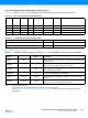
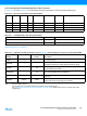
Writing any other combination than “10001”, “01001”, “00101”, “00011” or “00001” in the lower five bits will have
no effect.