
Data Sheet

252
ATmega48A/PA/88A/PA/168A/PA/328/P [DATASHEET]
Atmel-8271H-AVR- ATmega-Datasheet_08/2014
When ADCL is read, the ADC Data Register is not updated until ADCH is read. Consequently, if the result is left
adjusted and no more than 8-bit precision is required, it is sufficient to read ADCH. Otherwise, ADCL must be
read first, then ADCH.
The ADLAR bit in ADMUX, and the MUXn bits in ADMUX affect the way the result is read from the registers. If
ADLAR is set, the result is left adjusted. If ADLAR is cleared (default), the result is right adjusted.
• ADC9:0: ADC Conversion Result
These bits represent the result from the conversion, as detailed in ”ADC Conversion Result” on page 248.
24.9.4 ADCSRB – ADC Control and Status Register B
• Bit 7, 5:3 – Reserved
These bits are reserved for future use. To ensure compatibility with future devices, these bits must be written to
zero when ADCSRB is written.
• Bit 2:0 – ADTS[2:0]: ADC Auto Trigger Source
If ADATE in ADCSRA is written to one, the value of these bits selects which source will trigger an ADC
conversion. If ADATE is cleared, the ADTS[2:0] settings will have no effect. A conversion will be triggered by the
rising edge of the selected Interrupt Flag. Note that switching from a trigger source that is cleared to a trigger
source that is set, will generate a positive edge on the trigger signal. If ADEN in ADCSRA is set, this will start a
conversion. Switching to Free Running mode (ADTS[2:0]=0) will not cause a trigger event, even if the ADC
Interrupt Flag is set
.
24.9.5 DIDR0 – Digital Input Disable Register 0
• Bits 7:6 – Reserved
These bits are reserved for future use. To ensure compatibility with future devices, these bits must be written to
zero when DIDR0 is written.
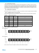
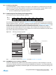
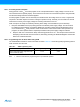
Bit 76543210
(0x7B) – ACME – – – ADTS2 ADTS1 ADTS0 ADCSRB
Read/Write R R/W R R R R/W R/W R/W
Initial Value 0 0 0 0 0 0 0 0
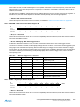
Table 24-6. ADC Auto Trigger Source Selections
ADTS2 ADTS1 ADTS0 Trigger Source
0 0 0 Free Running mode
0 0 1 Analog Comparator
0 1 0 External Interrupt Request 0
0 1 1 Timer/Counter0 Compare Match A
1 0 0 Timer/Counter0 Overflow
1 0 1 Timer/Counter1 Compare Match B
1 1 0 Timer/Counter1 Overflow
1 1 1 Timer/Counter1 Capture Event
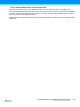
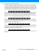
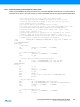
Bit 76543210
(0x7E) – – ADC5D ADC4D ADC3D ADC2D ADC1D ADC0D DIDR0
Read/Write R R R/W R/W R/W R/W R/W R/W
Initial Value 0 0 0 0 0 0 0 0