
Data Sheet

12
ATmega48A/PA/88A/PA/168A/PA/328/P [DATASHEET]
Atmel-8271H-AVR- ATmega-Datasheet_08/2014
Two 8-bit output operands and one 8-bit result input
Two 8-bit output operands and one 16-bit result input
One 16-bit output operand and one 16-bit result input
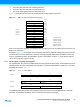
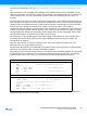
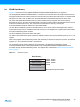
Figure 7-2 shows the structure of the 32 general purpose working registers in the CPU.
Figure 7-2. AVR CPU General Purpose Working Registers
Most of the instructions operating on the Register File have direct access to all registers, and most of them are
single cycle instructions.
As shown in Figure 7-2, each register is also assigned a data memory address, mapping them directly into the
first 32 locations of the user Data Space. Although not being physically implemented as SRAM locations, this
memory organization provides great flexibility in access of the registers, as the X-, Y- and Z-pointer registers
can be set to index any register in the file.
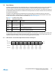
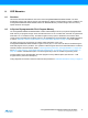
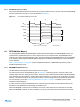
7.4.1 The X-register, Y-register, and Z-register
The registers R26...R31 have some added functions to their general purpose usage. These registers are 16-bit
address pointers for indirect addressing of the data space. The three indirect address registers X, Y, and Z are
defined as described in Figure 7-3.
Figure 7-3. The X-, Y-, and Z-registers
In the different addressing modes these address registers have functions as fixed displacement, automatic
increment, and automatic decrement (see the instruction set reference for details).
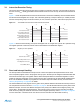
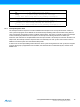
70Addr.
R0 0x00
R1 0x01
R2 0x02
…
R13 0x0D
General R14 0x0E
Purpose R15 0x0F
Working R16 0x10
Registers R17 0x11
…
R26 0x1A X-register Low Byte
R27 0x1B X-register High Byte
R28 0x1C Y-register Low Byte
R29 0x1D Y-register High Byte
R30 0x1E Z-register Low Byte
R31 0x1F Z-register High Byte
15 XH XL 0
X-register 7 0 7 0
R27 (0x1B) R26 (0x1A)
15 YH YL 0
Y-register 7 0 7 0
R29 (0x1D) R28 (0x1C)
15 ZH ZL 0
Z-register 7 0 7 0
R31 (0x1F) R30 (0x1E)