
Data Sheet

109
ATmega48A/PA/88A/PA/168A/PA/328/P [DATASHEET]
Atmel-8271H-AVR- ATmega-Datasheet_08/2014
If external pin modes are used for the Timer/Counter0, transitions on the T0 pin will clock the counter even if the
pin is configured as an output. This feature allows software control of the counting.
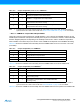
15.9.3 TCNT0 – Timer/Counter Register
The Timer/Counter Register gives direct access, both for read and write operations, to the Timer/Counter unit 8-
bit counter. Writing to the TCNT0 Register blocks (removes) the Compare Match on the following timer clock.
Modifying the counter (TCNT0) while the counter is running, introduces a risk of missing a Compare Match
between TCNT0 and the OCR0x Registers.
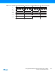
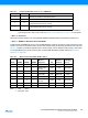
15.9.4 OCR0A – Output Compare Register A
The Output Compare Register A contains an 8-bit value that is continuously compared with the counter value
(TCNT0). A match can be used to generate an Output Compare interrupt, or to generate a waveform output on
the OC0A pin.
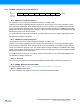
15.9.5 OCR0B – Output Compare Register B
The Output Compare Register B contains an 8-bit value that is continuously compared with the counter value
(TCNT0). A match can be used to generate an Output Compare interrupt, or to generate a waveform output on
the OC0B pin.
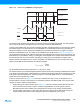
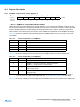
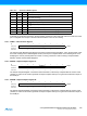
Table 15-9. Clock Select Bit Description
CS02 CS01 CS00 Description
0 0 0 No clock source (Timer/Counter stopped)
001clk
I/O
/(No prescaling)
010clk
I/O
/8 (From prescaler)
011clk
I/O
/64 (From prescaler)
100clk
I/O
/256 (From prescaler)
101clk
I/O
/1024 (From prescaler)
1 1 0 External clock source on T0 pin. Clock on falling edge.
1 1 1 External clock source on T0 pin. Clock on rising edge.
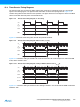
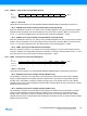
Bit 76543210
0x26 (0x46) TCNT0[7:0] TCNT0
Read/Write R/W R/W R/W R/W R/W R/W R/W R/W
Initial Value 0 0 0 0 0 0 0 0
Bit 76543210
0x27 (0x47) OCR0A[7:0] OCR0A
Read/Write R/W R/W R/W R/W R/W R/W R/W R/W
Initial Value 0 0 0 0 0 0 0 0
Bit 76543210
0x28 (0x48) OCR0B[7:0] OCR0B
Read/Write R/W R/W R/W R/W R/W R/W R/W R/W
Initial Value 0 0 0 0 0 0 0 0