ATmega48A/PA/88A/PA/168A/PA/328/P ATMEL 8-BIT MICROCONTROLLER WITH 4/8/16/32KB IN-SYSTEM PROGRAMMABLE FLASH DATASHEET Features High Performance, Low Power Atmel®AVR® 8-Bit Microcontroller Family Advanced RISC Architecture ̶ 131 Powerful Instructions – Most Single Clock Cycle Execution ̶ 32 x 8 General Purpose Working Registers ̶ Fully Static Operation ̶ Up to 20 MIPS Throughput at 20MHz ̶ On-chip 2-cycle Multiplier High Endurance Non-volatile Memory Segments ̶ 4/8/16/32KBytes of In-System Self-Pr
Special Microcontroller Features ̶ Power-on Reset and Programmable Brown-out Detection ̶ Internal Calibrated Oscillator ̶ External and Internal Interrupt Sources ̶ Six Sleep Modes: Idle, ADC Noise Reduction, Power-save, Power-down, Standby, and Extended Standby I/O and Packages ̶ 23 Programmable I/O Lines ̶ 28-pin PDIP, 32-lead TQFP, 28-pad QFN/MLF and 32-pad QFN/MLF Operating Voltage: ̶ 1.8 - 5.5V Temperature Range: ̶ -40C to 85C Speed Grade: ̶ 0 - 4MHz@1.8 - 5.5V, 0 - 10MHz@2.7 - 5.5.
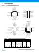
Pin Configurations Figure 1-1.
1.1 Pin Descriptions 1.1.1 VCC Digital supply voltage. 1.1.2 GND Ground. 1.1.3 Port B (PB7:0) XTAL1/XTAL2/TOSC1/TOSC2 Port B is an 8-bit bi-directional I/O port with internal pull-up resistors (selected for each bit). The Port B output buffers have symmetrical drive characteristics with both high sink and source capability. As inputs, Port B pins that are externally pulled low will source current if the pull-up resistors are activated.
1.1.7 AVCC AVCC is the supply voltage pin for the A/D Converter, PC3:0, and ADC7:6. It should be externally connected to VCC, even if the ADC is not used. If the ADC is used, it should be connected to VCC through a low-pass filter. Note that PC6...4 use digital supply voltage, VCC. 1.1.8 AREF AREF is the analog reference pin for the A/D Converter. 1.1.9 ADC7:6 (TQFP and QFN/MLF Package Only) In the TQFP and QFN/MLF package, ADC7:6 serve as analog inputs to the A/D converter.
2. Overview The ATmega48A/PA/88A/PA/168A/PA/328/P is a low-power CMOS 8-bit microcontroller based on the AVR enhanced RISC architecture. By executing powerful instructions in a single clock cycle, the ATmega48A/PA/88A/PA/168A/PA/328/P achieves throughputs approaching 1 MIPS per MHz allowing the system designer to optimize power consumption versus processing speed. Block Diagram VCC Block Diagram GND Figure 2-1.
The ATmega48A/PA/88A/PA/168A/PA/328/P provides the following features: 4K/8Kbytes of In-System Programmable Flash with Read-While-Write capabilities, 256/512/512/1Kbytes EEPROM, 512/1K/1K/2Kbytes SRAM, 23 general purpose I/O lines, 32 general purpose working registers, three flexible Timer/Counters with compare modes, internal and external interrupts, a serial programmable USART, a byte-oriented 2-wire Serial Interface, an SPI serial port, a 6-channel 10-bit ADC (8 channels in TQFP and QFN/MLF packages), a
ATmega48A/PA/88A/PA/168A/PA/328/P support a real Read-While-Write Self-Programming mechanism. There is a separate Boot Loader Section, and the SPM instruction can only execute from there. In ATmega 48A/48PA there is no Read-While-Write support and no separate Boot Loader Section. The SPM instruction can execute from the entire Flash 3. Resources A comprehensive set of development tools, application notes and datasheets are available for download on http://www.atmel.com/avr. Note: 4. 1.
7. AVR CPU Core 7.1 Overview This section discusses the AVR core architecture in general. The main function of the CPU core is to ensure correct program execution. The CPU must therefore be able to access memories, perform calculations, control peripherals, and handle interrupts. Figure 7-1.
operands are output from the Register File, the operation is executed, and the result is stored back in the Register File – in one clock cycle. Six of the 32 registers can be used as three 16-bit indirect address register pointers for Data Space addressing – enabling efficient address calculations. One of the these address pointers can also be used as an address pointer for look up tables in Flash program memory.
7.3.1 SREG – AVR Status Register The AVR Status Register – SREG – is defined as: Bit 7 6 5 4 3 2 1 0 0x3F (0x5F) I T H S V N Z C Read/Write R/W R/W R/W R/W R/W R/W R/W R/W Initial Value 0 0 0 0 0 0 0 0 SREG • Bit 7 – I: Global Interrupt Enable The Global Interrupt Enable bit must be set for the interrupts to be enabled. The individual interrupt enable control is then performed in separate control registers.
Two 8-bit output operands and one 8-bit result input Two 8-bit output operands and one 16-bit result input One 16-bit output operand and one 16-bit result input Figure 7-2 shows the structure of the 32 general purpose working registers in the CPU. Figure 7-2. AVR CPU General Purpose Working Registers 7 0 Addr.
7.5 Stack Pointer The Stack is mainly used for storing temporary data, for storing local variables and for storing return addresses after interrupts and subroutine calls. Note that the Stack is implemented as growing from higher to lower memory locations. The Stack Pointer Register always points to the top of the Stack. The Stack Pointer points to the data SRAM Stack area where the Subroutine and Interrupt Stacks are located. A Stack PUSH command will decrease the Stack Pointer.
7.6 Instruction Execution Timing This section describes the general access timing concepts for instruction execution. The AVR CPU is driven by the CPU clock clkCPU, directly generated from the selected clock source for the chip. No internal clock division is used. Figure 7-4 shows the parallel instruction fetches and instruction executions enabled by the Harvard architecture and the fast-access Register File concept.
programming the BOOTRST Fuse, see ”Boot Loader Support – Read-While-Write Self-Programming” on page 264. When an interrupt occurs, the Global Interrupt Enable I-bit is cleared and all interrupts are disabled. The user software can write logic one to the I-bit to enable nested interrupts. All enabled interrupts can then interrupt the current interrupt routine. The I-bit is automatically set when a Return from Interrupt instruction – RETI – is executed. There are basically two types of interrupts.
Assembly Code Example sei ; set Global Interrupt Enable sleep ; enter sleep, waiting for interrupt ; note: will enter sleep before any pending interrupt(s) C Code Example __enable_interrupt(); /* set Global Interrupt Enable */ __sleep(); /* enter sleep, waiting for interrupt */ /* note: will enter sleep before any pending interrupt(s) */ 7.7.1 Interrupt Response Time The interrupt execution response for all the enabled AVR interrupts is four clock cycles minimum.
8. AVR Memories 8.1 Overview This section describes the different memories in the ATmega48A/PA/88A/PA/168A/PA/328/P. The AVR architecture has two main memory spaces, the Data Memory and the Program Memory space. In addition, the ATmega48A/PA/88A/PA/168A/PA/328/P features an EEPROM Memory for data storage. All three memory spaces are linear and regular. 8.
Figure 8-1. Program Memory Map ATmega 48A/48PA Program Memory 0x0000 Application Flash Section 0x7FF Figure 8-2.
8.3 SRAM Data Memory Figure 8-3 shows how the ATmega48A/PA/88A/PA/168A/PA/328/P SRAM Memory is organized. The ATmega48A/PA/88A/PA/168A/PA/328/P is a complex microcontroller with more peripheral units than can be supported within the 64 locations reserved in the Opcode for the IN and OUT instructions. For the Extended I/O space from 0x60 - 0xFF in SRAM, only the ST/STS/STD and LD/LDS/LDD instructions can be used.
8.3.1 Data Memory Access Times This section describes the general access timing concepts for internal memory access. The internal data SRAM access is performed in two clkCPU cycles as described in Figure 8-4. Figure 8-4. On-chip Data SRAM Access Cycles T1 T2 T3 clkCPU Address Compute Address Address valid Write Data WR Read Data RD Memory Access Instruction 8.4 Next Instruction EEPROM Data Memory The ATmega48A/PA/88A/PA/168A/PA/328/P contains 256/512/512/1Kbytes of data EEPROM memory.
8.4.2 Preventing EEPROM Corruption During periods of low VCC, the EEPROM data can be corrupted because the supply voltage is too low for the CPU and the EEPROM to operate properly. These issues are the same as for board level systems using EEPROM, and the same design solutions should be applied. An EEPROM data corruption can be caused by two situations when the voltage is too low. First, a regular write sequence to the EEPROM requires a minimum voltage to operate correctly.
8.6 Register Description 8.6.
Table 8-1. EEPROM Mode Bits EEPM1 EEPM0 Programming Time 0 0 3.4ms Erase and Write in one operation (Atomic Operation) 0 1 1.8ms Erase Only 1 0 1.8ms Write Only 1 1 – Operation Reserved for future use • Bit 3 – EERIE: EEPROM Ready Interrupt Enable Writing EERIE to one enables the EEPROM Ready Interrupt if the I bit in SREG is set. Writing EERIE to zero disables the interrupt. The EEPROM Ready interrupt generates a constant interrupt when EEPE is cleared.
• Bit 0 – EERE: EEPROM Read Enable The EEPROM Read Enable Signal EERE is the read strobe to the EEPROM. When the correct address is set up in the EEAR Register, the EERE bit must be written to a logic one to trigger the EEPROM read. The EEPROM read access takes one instruction, and the requested data is available immediately. When the EEPROM is read, the CPU is halted for four cycles before the next instruction is executed. The user should poll the EEPE bit before starting the read operation.
Assembly Code Example EEPROM_write: ; Wait for completion of previous write sbic EECR,EEPE rjmp EEPROM_write ; Set up address (r18:r17) in address register out EEARH, r18 out EEARL, r17 ; Write data (r16) to Data Register out EEDR,r16 ; Write logical one to EEMPE sbi EECR,EEMPE ; Start eeprom write by setting EEPE sbi EECR,EEPE ret C Code Example void EEPROM_write(unsigned int uiAddress, unsigned char ucData) { /* Wait for completion of previous write */ while(EECR & (1<
EEPROM_read: ; Wait for completion of previous write sbic EECR,EEPE rjmp EEPROM_read ; Set up address (r18:r17) in address register out EEARH, r18 out EEARL, r17 ; Start eeprom read by writing EERE sbi EECR,EERE ; Read data from Data Register in r16,EEDR ret C Code Example unsigned char EEPROM_read(unsigned int uiAddress) { /* Wait for completion of previous write */ while(EECR & (1<
9. System Clock and Clock Options 9.1 Clock Systems and their Distribution Figure 9-1 presents the principal clock systems in the AVR and their distribution. All of the clocks need not be active at a given time. In order to reduce power consumption, the clocks to modules not being used can be halted by using different sleep modes, as described in ”Power Management and Sleep Modes” on page 40. The clock systems are detailed below. Figure 9-1.
9.1.3 Flash Clock – clkFLASH The Flash clock controls operation of the Flash interface. The Flash clock is usually active simultaneously with the CPU clock. 9.1.4 Asynchronous Timer Clock – clkASY The Asynchronous Timer clock allows the Asynchronous Timer/Counter to be clocked directly from an external clock or an external 32kHz clock crystal. The dedicated clock domain allows using this Timer/Counter as a realtime counter even when the device is in sleep mode. 9.1.
Table 9-2. Number of Watchdog Oscillator Cycles Typ Time-out (VCC = 5.0V) Typ Time-out (VCC = 3.0V) Number of Cycles 0ms 0ms 0 4.1ms 4.3ms 512 65ms 69ms 8K (8,192) Main purpose of the delay is to keep the AVR in reset until it is supplied with minimum VCC. The delay will not monitor the actual voltage and it will be required to select a delay longer than the VCC rise time. If this is not possible, an internal or external Brown-Out Detection circuit should be used.
Low Power Crystal Oscillator Operating Modes(3) Table 9-3. Frequency Range (MHz) Recommended Range for Capacitors C1 and C2 (pF) CKSEL3...1(1) 0.4 - 0.9 – 100(2) 0.9 - 3.0 12 - 22 101 3.0 - 8.0 12 - 22 110 8.0 - 16.0 12 - 22 111 Notes: 1. 2. 3. This is the recommended CKSEL settings for the difference frequency ranges. This option should not be used with crystals, only with ceramic resonators.
This Crystal Oscillator is a full swing oscillator, with rail-to-rail swing on the XTAL2 output. This is useful for driving other clock inputs and in noisy environments. The current consumption is higher than the ”Low Power Crystal Oscillator” on page 29. Note that the Full Swing Crystal Oscillator will only operate for VCC = 2.7 - 5.5 volts. C1 and C2 should always be equal for both crystals and resonators.
Table 9-6. Start-up Times for the Full Swing Crystal Oscillator Clock Selection (Continued) Start-up Time from Power-down and Power-save Additional Delay from Reset (VCC = 5.0V) CKSEL0 SUT1...0 Crystal Oscillator, BOD enabled 16K CK 14CK 1 01 Crystal Oscillator, fast rising power 16K CK 14CK + 4.1ms 1 10 Crystal Oscillator, slowly rising power 16K CK 14CK + 65ms 1 11 Oscillator Source / Power Conditions Notes: 1. 2.
9.5 Low Frequency Crystal Oscillator The Low-frequency Crystal Oscillator is optimized for use with a 32.768kHz watch crystal. When selecting crystals, load capacitance and crystal’s Equivalent Series Resistance, ESR must be taken into consideration. Both values are specified by the crystal vendor. ATmega48A/PA/88A/PA/168A/PA/328/P oscillator is optimized for very low power consumption, and thus when selecting crystals, see Table for maximum ESR recommendations on 6.5pF, 9.0pF and 12.
Table 9-10. Start-up Times for the Low-frequency Crystal Oscillator Clock Selection CKSEL3... 0 0100 Start-up Time from Power-down and Power-save (1) 1K CK 0101 Note: 9.6 1. Recommended Usage 32K CK Stable frequency at start-up This option should only be used if frequency stability at start-up is not important for the application Calibrated Internal RC Oscillator By default, the Internal RC Oscillator provides an approximate 8.0MHz clock.
9.7 128kHz Internal Oscillator The 128kHz internal Oscillator is a low power Oscillator providing a clock of 128kHz. The frequency is nominal at 3V and 25C. This clock may be select as the system clock by programming the CKSEL Fuses to “11” as shown in Table 9-13. Table 9-13. Note: 1. 128kHz Internal Oscillator Operating Modes Nominal Frequency(1) CKSEL3...0 128kHz 0011 Note that the 128kHz oscillator is a very low power clock source, and is not designed for high accuracy.
Table 9-16. Start-up Times for the External Clock Selection Start-up Time from Powerdown and Power-save Additional Delay from Reset (VCC = 5.0V) SUT1...0 BOD enabled 6 CK 14CK 00 Fast rising power 6 CK 14CK + 4.1ms 01 Slowly rising power 6 CK 14CK + 65ms 10 Power Conditions Reserved 11 When applying an external clock, it is required to avoid sudden changes in the applied clock frequency to ensure stable operation of the MCU.
From the time the CLKPS values are written, it takes between T1 + T2 and T1 + 2 * T2 before the new clock frequency is active. In this interval, 2 active clock edges are produced. Here, T1 is the previous clock period, and T2 is the period corresponding to the new prescaler setting. To avoid unintentional changes of clock frequency, a special write procedure must be followed to change the CLKPS bits: 1. Write the Clock Prescaler Change Enable (CLKPCE) bit to one and all other bits in CLKPR to zero. 2.
9.12 Register Description 9.12.1 OSCCAL – Oscillator Calibration Register Bit (0x66) Read/Write 7 6 5 4 3 2 1 0 CAL7 CAL6 CAL5 CAL4 CAL3 CAL2 CAL1 CAL0 R/W R/W R/W R/W R/W R/W R/W R/W Initial Value OSCCAL Device Specific Calibration Value • Bits 7:0 – CAL[7:0]: Oscillator Calibration Value The Oscillator Calibration Register is used to trim the Calibrated Internal RC Oscillator to remove process variations from the oscillator frequency.
Table 9-17.
10. Power Management and Sleep Modes Sleep modes enable the application to shut down unused modules in the MCU, thereby saving power. The AVR provides various sleep modes allowing the user to tailor the power consumption to the application’s requirements. When enabled, the Brown-out Detector (BOD) actively monitors the power supply voltage during the sleep periods. To further save power, it is possible to disable the BOD in some sleep modes. See ”BOD Disable(1)” on page 41 for more details. 10.
10.2 BOD Disable(1) When the Brown-out Detector (BOD) is enabled by BODLEVEL fuses - see Table 28-7 on page 283 and onwards, the BOD is actively monitoring the power supply voltage during a sleep period. To save power, it is possible to disable the BOD by software for some of the sleep modes, see Table 10-1 on page 40. The sleep mode power consumption will then be at the same level as when BOD is globally disabled by fuses.
INT0 or INT1, or a pin change interrupt can wake up the MCU. This sleep mode basically halts all generated clocks, allowing operation of asynchronous modules only. Note: If a level triggered interrupt is used for wake-up from Power-down, the required level must be held long enough for the MCU to complete the wake-up to trigger the level interrupt. If the level disappears before the end of the Start-up Time, the MCU will still wake up, but no interrupt will be generated. ”External Interrupts” on page 71.
10.8 Extended Standby Mode When the SM2...0 bits are 111 and an external crystal/resonator clock option is selected, the SLEEP instruction makes the MCU enter Extended Standby mode. This mode is identical to Power-save with the exception that the Oscillator is kept running. From Extended Standby mode, the device wakes up in six clock cycles. 10.
10.10.4 Internal Voltage Reference The Internal Voltage Reference will be enabled when needed by the Brown-out Detection, the Analog Comparator or the ADC. If these modules are disabled as described in the sections above, the internal voltage reference will be disabled and it will not be consuming power. When turned on again, the user must allow the reference to start up before the output is used. If the reference is kept on in sleep mode, the output can be used immediately.
10.11 Register Description 10.11.1 SMCR – Sleep Mode Control Register The Sleep Mode Control Register contains control bits for power management. Bit 7 6 5 4 3 2 1 0 0x33 (0x53) – – – – SM2 SM1 SM0 SE Read/Write R R R R R/W R/W R/W R/W Initial Value 0 0 0 0 0 0 0 0 SMCR • Bits [7:4]: Reserved These bits are unused in the ATmega48A/PA/88A/PA/168A/PA/328/P, and will always be read as zero.
10.11.2 MCUCR – MCU Control Register Bit 7 6 5 4 3 2 1 0 0x35 (0x55) – BODS(1) BODSE(1) PUD – – IVSEL IVCE Read/Write R R/W R/W R/W R R R/W R/W Initial Value 0 0 0 0 0 0 0 0 MCUCR • Bit 6 – BODS: BOD Sleep(1) The BODS bit must be written to logic one in order to turn off BOD during sleep, see Table 10-1 on page 40. Writing to the BODS bit is controlled by a timed sequence and an enable bit, BODSE in MCUCR.
• Bit 2 – PRSPI: Power Reduction Serial Peripheral Interface If using debugWIRE On-chip Debug System, this bit should not be written to one. Writing a logic one to this bit shuts down the Serial Peripheral Interface by stopping the clock to the module. When waking up the SPI again, the SPI should be re initialized to ensure proper operation. • Bit 1 – PRUSART0: Power Reduction USART0 Writing a logic one to this bit shuts down the USART by stopping the clock to the module.
11. System Control and Reset 11.1 Resetting the AVR During reset, all I/O Registers are set to their initial values, and the program starts execution from the Reset Vector. For ATmega168A/168PA/328/328P the instruction placed at the Reset Vector must be a JMP – Absolute Jump – instruction to the reset handling routine. For the ATmega 48A/48PA and ATmega88A/88PA, the instruction placed at the Reset Vector must be an RJMP – Relative Jump – instruction to the reset handling routine.
Figure 11-1. Reset Logic DATA BUS PORF BORF EXTRF WDRF MCU Status Register (MCUSR) Power-on Reset Circuit Brown-out Reset Circuit BODLEVEL [2..0] Pull-up Resistor SPIKE FILTER RSTDISBL Watchdog Oscillator Clock Generator CK Delay Counters TIMEOUT CKSEL[3:0] SUT[1:0] 11.3 Power-on Reset A Power-on Reset (POR) pulse is generated by an On-chip detection circuit. The detection level is defined in ”System and Reset Characteristics” on page 310.
Figure 11-3. MCU Start-up, RESET Extended Externally VCC VPOT RESET TIME-OUT VRST tTOUT INTERNAL RESET 11.4 External Reset An External Reset is generated by a low level on the RESET pin. Reset pulses longer than the minimum pulse width (see ”System and Reset Characteristics” on page 310) will generate a reset, even if the clock is not running. Shorter pulses are not guaranteed to generate a reset.
Figure 11-5. Brown-out Reset During Operation VCC VBOT- VBOT+ RESET tTOUT TIME-OUT INTERNAL RESET 11.6 Watchdog System Reset When the Watchdog times out, it will generate a short reset pulse of one CK cycle duration. On the falling edge of this pulse, the delay timer starts counting the Time-out period tTOUT. Refer to page 52 for details on operation of the Watchdog Timer. Figure 11-6. Watchdog System Reset During Operation CC CK 11.
11.8 Watchdog Timer 11.8.1 Features • Clocked from separate On-chip Oscillator • 3 Operating modes – Interrupt – System Reset – Interrupt and System Reset • Selectable Time-out period from 16ms to 8s • Possible Hardware fuse Watchdog always on (WDTON) for fail-safe mode 11.8.2 Overview ATmega48A/PA/88A/PA/168A/PA/328/P has an Enhanced Watchdog Timer (WDT). The WDT is a timer counting cycles of a separate on-chip 128kHz oscillator.
Assembly Code Example(1) WDT_off: ; Turn off global interrupt cli ; Reset Watchdog Timer wdr ; Clear WDRF in MCUSR in r16, MCUSR andi r16, ~(1<
The following code example shows one assembly and one C function for changing the time-out value of the Watchdog Timer. Assembly Code Example(1) WDT_Prescaler_Change: ; Turn off global interrupt cli ; Reset Watchdog Timer wdr ; Start timed sequence lds r16, WDTCSR ori r16, (1<
11.9 Register Description 11.9.1 MCUSR – MCU Status Register The MCU Status Register provides information on which reset source caused an MCU reset. Bit 7 6 5 4 3 2 1 0 0x34 (0x54) – – – – WDRF BORF EXTRF PORF Read/Write R R R R R/W R/W R/W R/W Initial Value 0 0 0 0 MCUSR See Bit Description • Bit 7:4: Reserved These bits are unused bits in the ATmega48A/PA/88A/PA/168A/PA/328/P, and will always read as zero.
the corresponding interrupt vector will clear WDIE and WDIF automatically by hardware (the Watchdog goes to System Reset Mode). This is useful for keeping the Watchdog Timer security while using the interrupt. To stay in Interrupt and System Reset Mode, WDIE must be set after each interrupt. This should however not be done within the interrupt service routine itself, as this might compromise the safety-function of the Watchdog System Reset mode.
Table 11-2. Watchdog Timer Prescale Select (Continued) WDP3 WDP2 WDP1 WDP0 1 0 1 0 1 0 1 1 1 1 0 0 1 1 0 1 1 1 1 0 1 1 1 1 Number of WDT Oscillator Cycles Typical Time-out at VCC = 5.
12. Interrupts This section describes the specifics of the interrupt handling as performed in ATmega48A/PA/88A/PA/168A/PA/328/P. For a general explanation of the AVR interrupt handling, refer to ”Reset and Interrupt Handling” on page 14. The interrupt vectors in ATmega 48A/48PA, ATmega88A/88PA, ATmega168A/168PA and ATmega328/328P are generally the same, with the following differences: 12.
Table 12-1. Reset and Interrupt Vectors in ATmega48A and ATmega48PA (Continued) Vector No.
12.2 Interrupt Vectors in ATmega88A and ATmega88PA Table 12-2. Reset and Interrupt Vectors in ATmega88A and ATmega88PA Vector No.
Reset and Interrupt Vectors Placement in ATmega88A and ATmega88PA(1) Table 12-3. BOOTRST IVSEL 1 Note: Reset Address Interrupt Vectors Start Address 0 0x000 0x001 1 1 0x000 Boot Reset Address + 0x001 0 0 Boot Reset Address 0x001 0 1 Boot Reset Address Boot Reset Address + 0x001 1. The Boot Reset Address is shown in Table 27-7 on page 276. For the BOOTRST Fuse “1” means unprogrammed while “0” means programmed.
0x002 0x003 0x004 0x005 ; .org 0xC01 0xC01 0xC02 ... 0xC19 ldi r16,low(RAMEND) out SPL,r16 sei ; Enable interrupts xxx rjmp rjmp ... rjmp EXT_INT0 EXT_INT1 ... SPM_RDY ; IRQ0 Handler ; IRQ1 Handler ; ; Store Program Memory Ready Handler When the BOOTRST Fuse is programmed and the Boot section size set to 2Kbytes, the most typical and general program setup for the Reset and Interrupt Vector Addresses in ATmega88A/88PA is: Address .org 0x001 0x001 0x002 ... 0x019 ; .
12.3 Interrupt Vectors in ATmega168A and ATmega168PA Table 12-4. Reset and Interrupt Vectors in ATmega168A and ATmega168PA VectorNo.
regular program code can be placed at these locations. This is also the case if the Reset Vector is in the Application section while the Interrupt Vectors are in the Boot section or vice versa. Reset and Interrupt Vectors Placement in ATmega168A and ATmega168PA(1) Table 12-5. BOOTRST IVSEL 1 Note: Reset Address Interrupt Vectors Start Address 0 0x000 0x002 1 1 0x000 Boot Reset Address + 0x0002 0 0 Boot Reset Address 0x002 0 1 Boot Reset Address Boot Reset Address + 0x0002 1.
Address Labels 0x0000 RESET: 0x0001 0x0002 0x0003 0x0004 0x0005 ; .org 0x1C02 0x1C02 0x1C04 ... 0x1C32 Code Comments ldi r16,high(RAMEND); Main program start out SPH,r16 ; Set Stack Pointer to top of RAM ldi r16,low(RAMEND) out SPL,r16 sei ; Enable interrupts xxx jmp jmp ... jmp EXT_INT0 EXT_INT1 ...
12.4 Interrupt Vectors in ATmega328 and ATmega328P Table 12-6. Reset and Interrupt Vectors in ATmega328 and ATmega328P VectorNo.
regular program code can be placed at these locations. This is also the case if the Reset Vector is in the Application section while the Interrupt Vectors are in the Boot section or vice versa. Reset and Interrupt Vectors Placement in ATmega328 and ATmega328P(1) Table 12-7. BOOTRST IVSEL 1 Note: Reset Address Interrupt Vectors Start Address 0 0x000 0x002 1 1 0x000 Boot Reset Address + 0x0002 0 0 Boot Reset Address 0x002 0 1 Boot Reset Address Boot Reset Address + 0x0002 1.
Address Labels 0x0000 RESET: 0x0001 0x0002 0x0003 0x0004 0x0005 ; .org 0x3C02 0x3C02 0x3C04 ... 0x3C32 Code Comments ldi r16,high(RAMEND); Main program start out SPH,r16 ; Set Stack Pointer to top of RAM ldi r16,low(RAMEND) out SPL,r16 sei ; Enable interrupts xxx jmp jmp ... jmp EXT_INT0 EXT_INT1 ...
12.5 Register Description 12.5.1 Moving Interrupts Between Application and Boot Space, ATmega88A/88PA, ATmega168A/168PA and ATmega328/328P The MCU Control Register controls the placement of the Interrupt Vector table. MCUCR – MCU Control Register Bit 7 6 5 4 3 2 1 0 0x35 (0x55) – BODS(1) BODSE(1) PUD – – IVSEL IVCE Read/Write R R/W R/W R/W R R R/W R/W Initial Value 0 0 0 0 0 0 0 0 Note: MCUCR 1.
Assembly Code Example Move_interrupts: ; Enable change of Interrupt Vectors ldi r16, (1<
13. External Interrupts The External Interrupts are triggered by the INT0 and INT1 pins or any of the PCINT23...0 pins. Observe that, if enabled, the interrupts will trigger even if the INT0 and INT1 or PCINT23...0 pins are configured as outputs. This feature provides a way of generating a software interrupt. The pin change interrupt PCI2 will trigger if any enabled PCINT[23:16] pin toggles. The pin change interrupt PCI1 will trigger if any enabled PCINT[14:8] pin toggles.
13.2 Register Description 13.2.1 EICRA – External Interrupt Control Register A The External Interrupt Control Register A contains control bits for interrupt sense control. Bit 7 6 5 4 3 2 1 0 (0x69) – – – – ISC11 ISC10 ISC01 ISC00 Read/Write R R R R R/W R/W R/W R/W Initial Value 0 0 0 0 0 0 0 0 EICRA • Bit 7:4 – Reserved These bits are unused bits in the ATmega48A/PA/88A/PA/168A/PA/328/P, and will always read as zero.
13.2.2 EIMSK – External Interrupt Mask Register Bit 7 6 5 4 3 2 1 0 0x1D (0x3D) – – – – – – INT1 INT0 Read/Write R R R R R R R/W R/W Initial Value 0 0 0 0 0 0 0 0 EIMSK • Bit 7:2 – Reserved These bits are unused bits in the ATmega48A/PA/88A/PA/168A/PA/328/P, and will always read as zero. • Bit 1 – INT1: External Interrupt Request 1 Enable When the INT1 bit is set (one) and the I-bit in the Status Register (SREG) is set (one), the external pin interrupt is enabled.
13.2.4 PCICR – Pin Change Interrupt Control Register Bit 7 6 5 4 3 2 1 0 (0x68) – – – – – PCIE2 PCIE1 PCIE0 Read/Write R R R R R R/W R/W R/W Initial Value 0 0 0 0 0 0 0 0 PCICR • Bit 7:3 – Reserved These bits are unused bits in the ATmega48A/PA/88A/PA/168A/PA/328/P, and will always read as zero. • Bit 2 – PCIE2: Pin Change Interrupt Enable 2 When the PCIE2 bit is set (one) and the I-bit in the Status Register (SREG) is set (one), pin change interrupt 2 is enabled.
• Bit 0 – PCIF0: Pin Change Interrupt Flag 0 When a logic change on any PCINT[7:0] pin triggers an interrupt request, PCIF0 becomes set (one). If the I-bit in SREG and the PCIE0 bit in PCICR are set (one), the MCU will jump to the corresponding Interrupt Vector. The flag is cleared when the interrupt routine is executed. Alternatively, the flag can be cleared by writing a logical one to it. 13.2.
14. I/O-Ports 14.1 Overview All AVR ports have true Read-Modify-Write functionality when used as general digital I/O ports. This means that the direction of one port pin can be changed without unintentionally changing the direction of any other pin with the SBI and CBI instructions. The same applies when changing drive value (if configured as output) or enabling/disabling of pull-up resistors (if configured as input).
14.2 Ports as General Digital I/O The ports are bi-directional I/O ports with optional internal pull-ups. Figure 14-2 shows a functional description of one I/O-port pin, here generically called Pxn. Figure 14-2.
14.2.3 Switching Between Input and Output When switching between tri-state ({DDxn, PORTxn} = 0b00) and output high ({DDxn, PORTxn} = 0b11), an intermediate state with either pull-up enabled {DDxn, PORTxn} = 0b01) or output low ({DDxn, PORTxn} = 0b10) must occur. Normally, the pull-up enabled state is fully acceptable, as a high-impedance environment will not notice the difference between a strong high driver and a pull-up.
signal transition on the pin will be delayed between ½ and 1½ system clock period depending upon the time of assertion. When reading back a software assigned pin value, a nop instruction must be inserted as indicated in Figure 144. The out instruction sets the “SYNC LATCH” signal at the positive edge of the clock. In this case, the delay tpd through the synchronizer is 1 system clock period. Figure 14-4.
Assembly Code Example(1) ... ; Define pull-ups and set outputs high ; Define directions for port pins ldi r16,(1<
The simplest method to ensure a defined level of an unused pin, is to enable the internal pull-up. In this case, the pull-up will be disabled during reset. If low power consumption during reset is important, it is recommended to use an external pull-up or pull-down. Connecting unused pins directly to VCC or GND is not recommended, since this may cause excessive currents if the pin is accidentally configured as an output.
Table 14-2 summarizes the function of the overriding signals. The pin and port indexes from Figure 14-5 on page 81 are not shown in the succeeding tables. The overriding signals are generated internally in the modules having the alternate function. Table 14-2. Generic Description of Overriding Signals for Alternate Functions Signal Name Full Name Description PUOE Pull-up Override Enable If this signal is set, the pull-up enable is controlled by the PUOV signal.
14.3.1 Alternate Functions of Port B The Port B pins with alternate functions are shown in Table 14-3. Table 14-3.
input of the inverting Oscillator amplifier. In this mode, a crystal Oscillator is connected to this pin, and the pin can not be used as an I/O pin. PCINT6: Pin Change Interrupt source 6. The PB6 pin can serve as an external interrupt source. If PB6 is used as a clock pin, DDB6, PORTB6 and PINB6 will all read 0. • SCK/PCINT5 – Port B, Bit 5 SCK: Master Clock output, Slave Clock input pin for SPI channel.
• ICP1/CLKO/PCINT0 – Port B, Bit 0 ICP1, Input Capture Pin: The PB0 pin can act as an Input Capture Pin for Timer/Counter1. CLKO, Divided System Clock: The divided system clock can be output on the PB0 pin. The divided system clock will be output if the CKOUT Fuse is programmed, regardless of the PORTB0 and DDB0 settings. It will also be output during reset. PCINT0: Pin Change Interrupt source 0. The PB0 pin can serve as an external interrupt source.
Table 14-5. Overriding Signals for Alternate Functions in PB3...
The alternate pin configuration is as follows: • RESET/PCINT14 – Port C, Bit 6 RESET, Reset pin: When the RSTDISBL Fuse is programmed, this pin functions as a normal I/O pin, and the part will have to rely on Power-on Reset and Brown-out Reset as its reset sources. When the RSTDISBL Fuse is unprogrammed, the reset circuitry is connected to the pin, and the pin can not be used as an I/O pin. If PC6 is used as a reset pin, DDC6, PORTC6 and PINC6 will all read 0. PCINT14: Pin Change Interrupt source 14.
• ADC1/PCINT9 – Port C, Bit 1 PC1 can also be used as ADC input Channel 1. Note that ADC input channel 1 uses analog power. PCINT9: Pin Change Interrupt source 9. The PC1 pin can serve as an external interrupt source. • ADC0/PCINT8 – Port C, Bit 0 PC0 can also be used as ADC input Channel 0. Note that ADC input channel 0 uses analog power. PCINT8: Pin Change Interrupt source 8. The PC0 pin can serve as an external interrupt source.
Table 14-8. Overriding Signals for Alternate Functions in PC3...
The alternate pin configuration is as follows: • AIN1/OC2B/PCINT23 – Port D, Bit 7 AIN1, Analog Comparator Negative Input. Configure the port pin as input with the internal pull-up switched off to avoid the digital port function from interfering with the function of the Analog Comparator. PCINT23: Pin Change Interrupt source 23. The PD7 pin can serve as an external interrupt source. • AIN0/OC0A/PCINT22 – Port D, Bit 6 AIN0, Analog Comparator Positive Input.
• RXD/PCINT16 – Port D, Bit 0 RXD, Receive Data (Data input pin for the USART). When the USART Receiver is enabled this pin is configured as an input regardless of the value of DDD0. When the USART forces this pin to be an input, the pull-up can still be controlled by the PORTD0 bit. PCINT16: Pin Change Interrupt source 16. The PD0 pin can serve as an external interrupt source. Table 14-10 and Table 14-11 relate the alternate functions of Port D to the overriding signals shown in Figure 14-5 on page 81.
14.4 Register Description 14.4.1 MCUCR – MCU Control Register Bit 7 6 5 4 3 2 1 0 0x35 (0x55) – BODS(1) BODSE(1) PUD – – IVSEL IVCE Read/Write R R/W R/W R/W R R R/W R/W Initial Value 0 0 0 0 0 0 0 0 Notes: MCUCR 1.
14.4.7 PINC – The Port C Input Pins Address(1) Bit 7 6 5 4 3 2 1 0 0x06 (0x26) – PINC6 PINC5 PINC4 PINC3 PINC2 PINC1 PINC0 Read/Write R R/W R/W R/W R/W R/W R/W R/W Initial Value 0 N/A N/A N/A N/A N/A N/A N/A PINC 14.4.8 PORTD – The Port D Data Register Bit 7 6 5 4 3 2 1 0 0x0B (0x2B) PORTD7 PORTD6 PORTD5 PORTD4 PORTD3 PORTD2 PORTD1 PORTD0 Read/Write R/W R/W R/W R/W R/W R/W R/W R/W Initial Value 0 0 0 0 0 0 0 0 PORTD 14.4.
15. 8-bit Timer/Counter0 with PWM 15.1 Features • • • • • • • Overview Timer/Counter0 is a general purpose 8-bit Timer/Counter module, with two independent Output Compare Units, and with PWM support. It allows accurate program execution timing (event management) and wave generation. A simplified block diagram of the 8-bit Timer/Counter is shown in Figure 15-1. For the actual placement of I/O pins, refer to ”Pinout ATmega48A/PA/88A/PA/168A/PA/328/P” on page 3.
15.2.1 Definitions Many register and bit references in this section are written in general form. A lower case “n” replaces the Timer/Counter number, in this case 0. A lower case “x” replaces the Output Compare Unit, in this case Compare Unit A or Compare Unit B. However, when using the register or bit defines in a program, the precise form must be used, i.e., TCNT0 for accessing Timer/Counter0 counter value and so on. The definitions in Table 15-1 are also used extensively throughout the document.
Figure 15-2. Counter Unit Block Diagram TOVn (Int.Req.) DATA BUS Clock Select count TCNTn clear Control Logic clkTn Edge Detector Tn direction ( From Prescaler ) bottom top Signal description (internal signals): count Increment or decrement TCNT0 by 1. direction Select between increment and decrement. clear Clear TCNT0 (set all bits to zero). clkTn Timer/Counter clock, referred to as clkT0 in the following. top Signalize that TCNT0 has reached maximum value.
Figure 15-3. Output Compare Unit, Block Diagram DATA BUS OCRnx TCNTn = (8-bit Comparator ) OCFnx (Int.Req.) top bottom Waveform Generator OCnx FOCn WGMn1:0 COMnx1:0 The OCR0x Registers are double buffered when using any of the Pulse Width Modulation (PWM) modes. For the normal and Clear Timer on Compare (CTC) modes of operation, the double buffering is disabled. The double buffering synchronizes the update of the OCR0x Compare Registers to either top or bottom of the counting sequence.
Be aware that the COM0x1:0 bits are not double buffered together with the compare value. Changing the COM0x1:0 bits will take effect immediately. 15.6 Compare Match Output Unit The Compare Output mode (COM0x1:0) bits have two functions. The Waveform Generator uses the COM0x1:0 bits for defining the Output Compare (OC0x) state at the next compare match. Also, the COM0x1:0 bits control the OC0x pin output source. Figure 15-4 shows a simplified schematic of the logic affected by the COM0x1:0 bit setting.
15.7 Modes of Operation The mode of operation, i.e., the behavior of the Timer/Counter and the Output Compare pins, is defined by the combination of the Waveform Generation mode (WGM02:0) and Compare Output mode (COM0x1:0) bits. The Compare Output mode bits do not affect the counting sequence, while the Waveform Generation mode bits do. The COM0x1:0 bits control whether the PWM output generated should be inverted or not (inverted or noninverted PWM).
For generating a waveform output in CTC mode, the OC0A output can be set to toggle its logical level on each compare match by setting the Compare Output mode bits to toggle mode (COM0A1:0 = 1). The OC0A value will not be visible on the port pin unless the data direction for the pin is set to output. The waveform generated will have a maximum frequency of fOC0 = fclk_I/O/2 when OCR0A is set to zero (0x00).
setting the COM0x1:0 to three: Setting the COM0A1:0 bits to one allows the OC0A pin to toggle on Compare Matches if the WGM02 bit is set. This option is not available for the OC0B pin (see Table 15-6 on page 106). The actual OC0x value will only be visible on the port pin if the data direction for the port pin is set as output.
Figure 15-7. Phase Correct PWM Mode, Timing Diagram OCnx Interrupt Flag Set OCRnx Update TOVn Interrupt Flag Set TCNTn OCnx (COMnx1:0 = 2) OCnx (COMnx1:0 = 3) Period 1 2 3 The Timer/Counter Overflow Flag (TOV0) is set each time the counter reaches BOTTOM. The Interrupt Flag can be used to generate an interrupt each time the counter reaches the BOTTOM value. In phase correct PWM mode, the compare unit allows generation of PWM waveforms on the OC0x pins.
15.8 Timer/Counter Timing Diagrams The Timer/Counter is a synchronous design and the timer clock (clkT0) is therefore shown as a clock enable signal in the following figures. The figures include information on when interrupt flags are set. Figure 15-8 contains timing data for basic Timer/Counter operation. The figure shows the count sequence close to the MAX value in all modes other than phase correct PWM mode. Figure 15-8.
Figure 15-11.
15.9 Register Description 15.9.1 TCCR0A – Timer/Counter Control Register A Bit 7 6 5 4 3 2 1 0 0x24 (0x44) COM0A1 COM0A0 COM0B1 COM0B0 – – WGM01 WGM00 Read/Write R/W R/W R/W R/W R R R/W R/W Initial Value 0 0 0 0 0 0 0 0 TCCR0A • Bits 7:6 – COM0A1:0: Compare Match Output A Mode These bits control the Output Compare pin (OC0A) behavior. If one or both of the COM0A1:0 bits are set, the OC0A output overrides the normal port functionality of the I/O pin it is connected to.
Table 15-4. Compare Output Mode, Phase Correct PWM Mode(1) COM0A1 COM0A0 0 0 Normal port operation, OC0A disconnected. 0 1 WGM02 = 0: Normal Port Operation, OC0A Disconnected. WGM02 = 1: Toggle OC0A on Compare Match. 1 0 Clear OC0A on Compare Match when up-counting. Set OC0A on Compare Match when down-counting. 1 1 Set OC0A on Compare Match when up-counting. Clear OC0A on Compare Match when down-counting. Note: 1. Description A special case occurs when OCR0A equals TOP and COM0A1 is set.
Compare Output Mode, Phase Correct PWM Mode(1) Table 15-7. COM0B1 COM0B0 0 0 Normal port operation, OC0B disconnected. 0 1 Reserved 1 0 Clear OC0B on Compare Match when up-counting. Set OC0B on Compare Match when down-counting. 1 1 Set OC0B on Compare Match when up-counting. Clear OC0B on Compare Match when down-counting. Note: 1. Description A special case occurs when OCR0B equals TOP and COM0B1 is set. In this case, the Compare Match is ignored, but the set or clear is done at TOP.
15.9.2 TCCR0B – Timer/Counter Control Register B Bit 7 6 5 4 3 2 1 0 0x25 (0x45) FOC0A FOC0B – – WGM02 CS02 CS01 CS00 Read/Write W W R R R/W R/W R/W R/W Initial Value 0 0 0 0 0 0 0 0 TCCR0B • Bit 7 – FOC0A: Force Output Compare A The FOC0A bit is only active when the WGM bits specify a non-PWM mode. However, for ensuring compatibility with future devices, this bit must be set to zero when TCCR0B is written when operating in PWM mode.
Table 15-9. Clock Select Bit Description CS02 CS01 CS00 Description 0 0 0 No clock source (Timer/Counter stopped) 0 0 1 clkI/O/(No prescaling) 0 1 0 clkI/O/8 (From prescaler) 0 1 1 clkI/O/64 (From prescaler) 1 0 0 clkI/O/256 (From prescaler) 1 0 1 clkI/O/1024 (From prescaler) 1 1 0 External clock source on T0 pin. Clock on falling edge. 1 1 1 External clock source on T0 pin. Clock on rising edge.
15.9.6 TIMSK0 – Timer/Counter Interrupt Mask Register Bit 7 6 5 4 3 2 1 0 (0x6E) – – – – – OCIE0B OCIE0A TOIE0 Read/Write R R R R R R/W R/W R/W Initial Value 0 0 0 0 0 0 0 0 TIMSK0 • Bits 7:3 – Reserved These bits are reserved bits in the ATmega48A/PA/88A/PA/168A/PA/328/P and will always read as zero.
• Bit 0 – TOV0: Timer/Counter0 Overflow Flag The bit TOV0 is set when an overflow occurs in Timer/Counter0. TOV0 is cleared by hardware when executing the corresponding interrupt handling vector. Alternatively, TOV0 is cleared by writing a logic one to the flag. When the SREG I-bit, TOIE0 (Timer/Counter0 Overflow Interrupt Enable), and TOV0 are set, the Timer/Counter0 Overflow interrupt is executed. The setting of this flag is dependent of the WGM02:0 bit setting.
16. 16-bit Timer/Counter1 with PWM 16.1 Features • • • • • • • • • • • 16.2 True 16-bit Design (i.e.
Figure 16-1. 16-bit Timer/Counter Block Diagram(1) Count Clear Direction TOVn (Int.Req.) Control Logic clkTn Clock Select Edge Detector TOP Tn BOTTOM ( From Prescaler ) Timer/Counter TCNTn = =0 OCnA (Int.Req.) Waveform Generation = OCnA DATA BUS OCRnA OCnB (Int.Req.) Fixed TOP Values Waveform Generation = OCRnB OCnB ( From Analog Comparator Ouput ) ICFn (Int.Req.) Edge Detector ICRn Noise Canceler ICPn TCCRnA Note: TCCRnB 1.
The Input Capture unit includes a digital filtering unit (Noise Canceler) for reducing the chance of capturing noise spikes. The TOP value, or maximum Timer/Counter value, can in some modes of operation be defined by either the OCR1A Register, the ICR1 Register, or by a set of fixed values. When using OCR1A as TOP value in a PWM mode, the OCR1A Register can not be used for generating a PWM output. However, the TOP value will in this case be double buffered allowing the TOP value to be changed in run time.
Assembly Code Examples(1) ... ; Set TCNT1 to 0x01FF ldi r17,0x01 ldi r16,0xFF out TCNT1H,r17 out TCNT1L,r16 ; Read TCNT1 into r17:r16 in r16,TCNT1L in r17,TCNT1H ... C Code Examples(1) unsigned int i; ... /* Set TCNT1 to 0x01FF */ TCNT1 = 0x1FF; /* Read TCNT1 into i */ i = TCNT1; ... Note: 1. See ”About Code Examples” on page 8. For I/O Registers located in extended I/O map, “IN”, “OUT”, “SBIS”, “SBIC”, “CBI”, and “SBI” instructions must be replaced with instructions that allow access to extended I/O.
Assembly Code Example(1) TIM16_ReadTCNT1: ; Save global interrupt flag in r18,SREG ; Disable interrupts cli ; Read TCNT1 into r17:r16 in r16,TCNT1L in r17,TCNT1H ; Restore global interrupt flag out SREG,r18 ret C Code Example(1) unsigned int TIM16_ReadTCNT1( void ) { unsigned char sreg; unsigned int i; /* Save global interrupt flag */ sreg = SREG; /* Disable interrupts */ _CLI(); /* Read TCNT1 into i */ i = TCNT1; /* Restore global interrupt flag */ SREG = sreg; return i; } Note: 1.
Assembly Code Example(1) TIM16_WriteTCNT1: ; Save global interrupt flag in r18,SREG ; Disable interrupts cli ; Set TCNT1 to r17:r16 out TCNT1H,r17 out TCNT1L,r16 ; Restore global interrupt flag out SREG,r18 ret C Code Example(1) void TIM16_WriteTCNT1( unsigned int i ) { unsigned char sreg; unsigned int i; /* Save global interrupt flag */ sreg = SREG; /* Disable interrupts */ _CLI(); /* Set TCNT1 to i */ TCNT1 = i; /* Restore global interrupt flag */ SREG = sreg; } Note: 1.
Figure 16-2. Counter Unit Block Diagram DATA BUS (8-bit) TOVn (Int.Req.) TEMP (8-bit) Clock Select Count TCNTnH (8-bit) TCNTnL (8-bit) TCNTn (16-bit Counter) Clear Direction Control Logic Edge Detector clkTn Tn ( From Prescaler ) TOP BOTTOM Signal description (internal signals): Count Increment or decrement TCNT1 by 1. Direction Select between increment and decrement. Clear Clear TCNT1 (set all bits to zero). clkT1 Timer/Counter clock.
The Input Capture unit is illustrated by the block diagram shown in Figure 16-3. The elements of the block diagram that are not directly a part of the Input Capture unit are gray shaded. The small “n” in register and bit names indicates the Timer/Counter number. Figure 16-3.
four system clock cycles. Note that the input of the noise canceler and edge detector is always enabled unless the Timer/Counter is set in a Waveform Generation mode that uses ICR1 to define TOP. An Input Capture can be triggered by software by controlling the port of the ICP1 pin. 16.6.2 Noise Canceler The noise canceler improves noise immunity by using a simple digital filtering scheme.
Figure 16-4. Output Compare Unit, Block Diagram DATA BUS (8-bit) TEMP (8-bit) OCRnxH Buf. (8-bit) OCRnxL Buf. (8-bit) TCNTnH (8-bit) OCRnx Buffer (16-bit Register) OCRnxH (8-bit) TCNTnL (8-bit) TCNTn (16-bit Counter) OCRnxL (8-bit) OCRnx (16-bit Register) = (16-bit Comparator ) OCFnx (Int.Req.) TOP BOTTOM Waveform Generator WGMn3:0 OCnx COMnx1:0 The OCR1x Register is double buffered when using any of the twelve Pulse Width Modulation (PWM) modes.
16.7.3 Using the Output Compare Unit Since writing TCNT1 in any mode of operation will block all compare matches for one timer clock cycle, there are risks involved when changing TCNT1 when using any of the Output Compare channels, independent of whether the Timer/Counter is running or not. If the value written to TCNT1 equals the OCR1x value, the compare match will be missed, resulting in incorrect waveform generation. Do not write the TCNT1 equal to TOP in PWM modes with variable TOP values.
must be set as output before the OC1x value is visible on the pin. The port override function is generally independent of the Waveform Generation mode, but there are some exceptions. Refer to Table 16-1 on page 132, Table 16-2 on page 132 and Table 16-3 on page 133 for details. The design of the Output Compare pin logic allows initialization of the OC1x state before the output is enabled. Note that some COM1x1:0 bit settings are reserved for certain modes of operation.
The timing diagram for the CTC mode is shown in Figure 16-6. The counter value (TCNT1) increases until a compare match occurs with either OCR1A or ICR1, and then counter (TCNT1) is cleared. Figure 16-6.
The PWM resolution for fast PWM can be fixed to 8-, 9-, or 10-bit, or defined by either ICR1 or OCR1A. The minimum resolution allowed is 2-bit (ICR1 or OCR1A set to 0x0003), and the maximum resolution is 16-bit (ICR1 or OCR1A set to MAX).
actively changed (by changing the TOP value), using the OCR1A as TOP is clearly a better choice due to its double buffer feature. In fast PWM mode, the compare units allow generation of PWM waveforms on the OC1x pins. Setting the COM1x1:0 bits to three will produce a inverted PWM and an non-inverted PWM output can be generated by setting the COM1x1:0 to two (see Table 16-2 on page 132).
the TCNT1 slopes represent compare matches between OCR1x and TCNT1. The OC1x Interrupt Flag will be set when a compare match occurs. Figure 16-8. Phase Correct PWM Mode, Timing Diagram OCRnx/TOP Update and OCnA Interrupt Flag Set or ICFn Interrupt Flag Set (Interrupt on TOP) TOVn Interrupt Flag Set (Interrupt on Bottom) TCNTn OCnx (COMnx1:0 = 2) OCnx (COMnx1:0 = 3) Period 1 2 3 4 The Timer/Counter Overflow Flag (TOV1) is set each time the counter reaches BOTTOM.
The N variable represents the prescaler divider (1, 8, 64, 256, or 1024). The extreme values for the OCR1x Register represent special cases when generating a PWM waveform output in the phase correct PWM mode. If the OCR1x is set equal to BOTTOM the output will be continuously low and if set equal to TOP the output will be continuously high for non-inverted PWM mode. For inverted PWM the output will have the opposite logic values.
Figure 16-9. Phase and Frequency Correct PWM Mode, Timing Diagram OCnA Interrupt Flag Set or ICFn Interrupt Flag Set (Interrupt on TOP) OCRnx/TOP Updateand TOVn Interrupt Flag Set (Interrupt on Bottom) TCNTn OCnx (COMnx1:0 = 2) OCnx (COMnx1:0 = 3) Period 1 2 3 4 The Timer/Counter Overflow Flag (TOV1) is set at the same timer clock cycle as the OCR1x Registers are updated with the double buffer value (at BOTTOM).
output will have the opposite logic values. If OCR1A is used to define the TOP value (WGM13:0 = 9) and COM1A1:0 = 1, the OC1A output will toggle with a 50% duty cycle. 16.10 Timer/Counter Timing Diagrams The Timer/Counter is a synchronous design and the timer clock (clkT1) is therefore shown as a clock enable signal in the following figures.
Figure 16-12. Timer/Counter Timing Diagram, no Prescaling. clkI/O clkTn (clkI/O /1) TCNTn (CTC and FPWM) TCNTn (PC and PFC PWM) TOP - 1 TOP BOTTOM BOTTOM + 1 TOP - 1 TOP TOP - 1 TOP - 2 TOVn (FPWM) and ICFn (if used as TOP) OCRnx (Update at TOP) New OCRnx Value Old OCRnx Value Figure 16-13 shows the same timing data, but with the prescaler enabled. Figure 16-13.
16.11 Register Description 16.11.1 TCCR1A – Timer/Counter1 Control Register A Bit 7 6 5 4 3 2 1 0 COM1A1 COM1A0 COM1B1 COM1B0 – – WGM11 WGM10 Read/Write R/W R/W R/W R/W R R R/W R/W Initial Value 0 0 0 0 0 0 0 0 (0x80) TCCR1A • Bit 7:6 – COM1A1:0: Compare Output Mode for Channel A • Bit 5:4 – COM1B1:0: Compare Output Mode for Channel B The COM1A1:0 and COM1B1:0 control the Output Compare pins (OC1A and OC1B respectively) behavior.
Table 16-3 shows the COM1x1:0 bit functionality when the WGM13:0 bits are set to the phase correct or the phase and frequency correct, PWM mode. Compare Output Mode, Phase Correct and Phase and Frequency Correct PWM(1) Table 16-3. COM1A1/COM1B1 COM1A0/COM1B0 0 0 Normal port operation, OC1A/OC1B disconnected. 0 1 WGM13:0 = 9 or 11: Toggle OC1A on Compare Match, OC1B disconnected (normal port operation). For all other WGM1 settings, normal port operation, OC1A/OC1B disconnected.
Waveform Generation Mode Bit Description(1) (Continued) Table 16-4. Timer/Counter Mode of Operation TOP Update of OCR1x at TOV1 Flag Set on 1 (Reserved) – – – 1 0 Fast PWM ICR1 BOTTOM TOP 1 1 Fast PWM OCR1A BOTTOM TOP Mode WGM13 WGM12 (CTC1) WGM11 (PWM11) WGM10 (PWM10) 13 1 1 0 14 1 1 15 1 1 Note: 1. The CTC1 and PWM11:0 bit definition names are obsolete. Use the WGM12:0 definitions.
Table 16-5. Clock Select Bit Description CS12 CS11 CS10 Description 0 0 0 No clock source (Timer/Counter stopped). 0 0 1 clkI/O/1 (No prescaling) 0 1 0 clkI/O/8 (From prescaler) 0 1 1 clkI/O/64 (From prescaler) 1 0 0 clkI/O/256 (From prescaler) 1 0 1 clkI/O/1024 (From prescaler) 1 1 0 External clock source on T1 pin. Clock on falling edge. 1 1 1 External clock source on T1 pin. Clock on rising edge.
16.11.5 OCR1AH and OCR1AL – Output Compare Register 1 A Bit 7 6 5 4 3 (0x89) OCR1A[15:8] (0x88) OCR1A[7:0] 2 1 0 OCR1AH OCR1AL Read/Write R/W R/W R/W R/W R/W R/W R/W R/W Initial Value 0 0 0 0 0 0 0 0 2 1 0 16.11.
• Bit 4, 3 – Reserved These bits are unused bits in the ATmega48A/PA/88A/PA/168A/PA/328/P, and will always read as zero. • Bit 2 – OCIE1B: Timer/Counter1, Output Compare B Match Interrupt Enable When this bit is written to one, and the I-flag in the Status Register is set (interrupts globally enabled), the Timer/Counter1 Output Compare B Match interrupt is enabled. The corresponding Interrupt Vector (see “Interrupts” on page 58) is executed when the OCF1B Flag, located in TIFR1, is set.
OCF1A is automatically cleared when the Output Compare Match A Interrupt Vector is executed. Alternatively, OCF1A can be cleared by writing a logic one to its bit location. • Bit 0 – TOV1: Timer/Counter1, Overflow Flag The setting of this flag is dependent of the WGM13:0 bits setting. In Normal and CTC modes, the TOV1 Flag is set when the timer overflows. Refer to Table 16-4 on page 133 for the TOV1 Flag behavior when using another WGM13:0 bit setting.
17. Timer/Counter0 and Timer/Counter1 Prescalers ”8-bit Timer/Counter0 with PWM” on page 94 and ”16-bit Timer/Counter1 with PWM” on page 112 share the same prescaler module, but the Timer/Counters can have different prescaler settings. The description below applies to both Timer/Counter1 and Timer/Counter0. 17.1 Internal Clock Source The Timer/Counter can be clocked directly by the system clock (by setting the CSn2:0 = 1).
fclk_I/O/2) given a 50/50% duty cycle. Since the edge detector uses sampling, the maximum frequency of an external clock it can detect is half the sampling frequency (Nyquist sampling theorem). However, due to variation of the system clock frequency and duty cycle caused by Oscillator source (crystal, resonator, and capacitors) tolerances, it is recommended that maximum frequency of an external clock source is less than fclk_I/O/2.5. An external clock source can not be prescaled. Figure 17-2.
17.4 Register Description 17.4.1 GTCCR – General Timer/Counter Control Register Bit 7 6 5 4 3 2 1 0 0x23 (0x43) TSM – – – – – PSRASY PSRSYNC Read/Write R/W R R R R R R/W R/W Initial Value 0 0 0 0 0 0 0 0 GTCCR • Bit 7 – TSM: Timer/Counter Synchronization Mode Writing the TSM bit to one activates the Timer/Counter Synchronization mode.
18. 8-bit Timer/Counter2 with PWM and Asynchronous Operation 18.1 Features • • • • • • • 18.2 Single Channel Counter Clear Timer on Compare Match (Auto Reload) Glitch-free, Phase Correct Pulse Width Modulator (PWM) Frequency Generator 10-bit Clock Prescaler Overflow and Compare Match Interrupt Sources (TOV2, OCF2A and OCF2B) Allows Clocking from External 32kHz Watch Crystal Independent of the I/O Clock Overview Timer/Counter2 is a general purpose, single channel, 8-bit Timer/Counter module.
individually masked with the Timer Interrupt Mask Register (TIMSK2). TIFR2 and TIMSK2 are not shown in the figure. The Timer/Counter can be clocked internally, via the prescaler, or asynchronously clocked from the TOSC1/2 pins, as detailed later in this section. The asynchronous operation is controlled by the Asynchronous Status Register (ASSR). The Clock Select logic block controls which clock source he Timer/Counter uses to increment (or decrement) its value.
Signal description (internal signals): count Increment or decrement TCNT2 by 1. direction Selects between increment and decrement. clear Clear TCNT2 (set all bits to zero). clkTn Timer/Counter clock, referred to as clkT2 in the following. top Signalizes that TCNT2 has reached maximum value. bottom Signalizes that TCNT2 has reached minimum value (zero). Depending on the mode of operation used, the counter is cleared, incremented, or decremented at each timer clock (clkT2).
Figure 18-3. Output Compare Unit, Block Diagram DATA BUS OCRnx TCNTn = (8-bit Comparator ) OCFnx (Int.Req.) top bottom Waveform Generator OCnx FOCn WGMn1:0 COMnX1:0 The OCR2x Register is double buffered when using any of the Pulse Width Modulation (PWM) modes. For the Normal and Clear Timer on Compare (CTC) modes of operation, the double buffering is disabled. The double buffering synchronizes the update of the OCR2x Compare Register to either top or bottom of the counting sequence.
18.6 Compare Match Output Unit The Compare Output mode (COM2x1:0) bits have two functions. The Waveform Generator uses the COM2x1:0 bits for defining the Output Compare (OC2x) state at the next compare match. Also, the COM2x1:0 bits control the OC2x pin output source. Figure 18-4 shows a simplified schematic of the logic affected by the COM2x1:0 bit setting. The I/O Registers, I/O bits, and I/O pins in the figure are shown in bold.
18.7 Modes of Operation The mode of operation, i.e., the behavior of the Timer/Counter and the Output Compare pins, is defined by the combination of the Waveform Generation mode (WGM22:0) and Compare Output mode (COM2x1:0) bits. The Compare Output mode bits do not affect the counting sequence, while the Waveform Generation mode bits do. The COM2x1:0 bits control whether the PWM output generated should be inverted or not (inverted or noninverted PWM).
For generating a waveform output in CTC mode, the OC2A output can be set to toggle its logical level on each compare match by setting the Compare Output mode bits to toggle mode (COM2A1:0 = 1). The OC2A value will not be visible on the port pin unless the data direction for the pin is set to output. The waveform generated will have a maximum frequency of fOC2A = fclk_I/O/2 when OCR2A is set to zero (0x00).
In fast PWM mode, the compare unit allows generation of PWM waveforms on the OC2x pin. Setting the COM2x1:0 bits to two will produce a non-inverted PWM and an inverted PWM output can be generated by setting the COM2x1:0 to three. TOP is defined as 0xFF when WGM2:0 = 3, and OCR2A when MGM2:0 = 7. (See Table 18-3 on page 154). The actual OC2x value will only be visible on the port pin if the data direction for the port pin is set as output.
Figure 18-7. Phase Correct PWM Mode, Timing Diagram OCnx Interrupt Flag Set OCRnx Update TOVn Interrupt Flag Set TCNTn OCnx (COMnx1:0 = 2) OCnx (COMnx1:0 = 3) Period 1 2 3 The Timer/Counter Overflow Flag (TOV2) is set each time the counter reaches BOTTOM. The Interrupt Flag can be used to generate an interrupt each time the counter reaches the BOTTOM value. In phase correct PWM mode, the compare unit allows generation of PWM waveforms on the OC2x pin.
18.8 Timer/Counter Timing Diagrams The following figures show the Timer/Counter in synchronous mode, and the timer clock (clkT2) is therefore shown as a clock enable signal. In asynchronous mode, clkI/O should be replaced by the Timer/Counter Oscillator clock. The figures include information on when Interrupt Flags are set. Figure 18-8 contains timing data for basic Timer/Counter operation. The figure shows the count sequence close to the MAX value in all modes other than phase correct PWM mode.
Figure 18-11. Timer/Counter Timing Diagram, Clear Timer on Compare Match mode, with Prescaler (fclk_I/O/8) clkI/O clkTn (clkI/O /8) TCNTn (CTC) TOP - 1 TOP BOTTOM BOTTOM + 1 TOP OCRnx OCFnx 18.9 Asynchronous Operation of Timer/Counter2 When Timer/Counter2 operates asynchronously, some considerations must be taken. Warning: When switching between asynchronous and synchronous clocking of Timer/Counter2, the Timer Registers TCNT2, OCR2x, and TCCR2x might be corrupted.
second to stabilize. The user is advised to wait for at least one second before using Timer/Counter2 after power-up or wake-up from Power-down or Standby mode. The contents of all Timer/Counter2 Registers must be considered lost after a wake-up from Power-down or Standby mode due to unstable clock signal upon start-up, no matter whether the Oscillator is in use or a clock signal is applied to the TOSC1 pin.
are disconnected from Port B. A crystal can then be connected between the TOSC1 and TOSC2 pins to serve as an independent clock source for Timer/Counter2. The Oscillator is optimized for use with a 32.768kHz crystal. For Timer/Counter2, the possible prescaled selections are: clkT2S/8, clkT2S/32, clkT2S/64, clkT2S/128, clkT2S/256, and clkT2S/1024. Additionally, clkT2S as well as 0 (stop) may be selected. Setting the PSRASY bit in GTCCR resets the prescaler.
Table 18-4 shows the COM2A1:0 bit functionality when the WGM22:0 bits are set to phase correct PWM mode. Table 18-4. Compare Output Mode, Phase Correct PWM Mode(1) COM2A1 COM2A0 0 0 Normal port operation, OC2A disconnected. 0 1 WGM22 = 0: Normal Port Operation, OC2A Disconnected. WGM22 = 1: Toggle OC2A on Compare Match. 1 0 Clear OC2A on Compare Match when up-counting. Set OC2A on Compare Match when down-counting. 1 1 Set OC2A on Compare Match when up-counting.
Table 18-7 shows the COM2B1:0 bit functionality when the WGM22:0 bits are set to phase correct PWM mode. Table 18-7. Compare Output Mode, Phase Correct PWM Mode(1) COM2B1 COM2B0 0 0 Normal port operation, OC2B disconnected. 0 1 Reserved 1 0 Clear OC2B on Compare Match when up-counting. Set OC2B on Compare Match when down-counting. 1 1 Set OC2B on Compare Match when up-counting. Clear OC2B on Compare Match when down-counting. Note: 1.
18.11.2 TCCR2B – Timer/Counter Control Register B Bit 7 6 5 4 3 2 1 0 FOC2A FOC2B – – WGM22 CS22 CS21 CS20 Read/Write W W R R R/W R/W R/W R/W Initial Value 0 0 0 0 0 0 0 0 (0xB1) TCCR2B • Bit 7 – FOC2A: Force Output Compare A The FOC2A bit is only active when the WGM bits specify a non-PWM mode. However, for ensuring compatibility with future devices, this bit must be set to zero when TCCR2B is written when operating in PWM mode.
Table 18-9. Clock Select Bit Description CS22 CS21 CS20 Description 1 0 1 clkT2S/128 (From prescaler) 1 1 0 clkT2S/256 (From prescaler) 1 1 1 clkT2S/1024 (From prescaler) If external pin modes are used for the Timer/Counter0, transitions on the T0 pin will clock the counter even if the pin is configured as an output. This feature allows software control of the counting. 18.11.
• Bit 1 – OCIE2A: Timer/Counter2 Output Compare Match A Interrupt Enable When the OCIE2A bit is written to one and the I-bit in the Status Register is set (one), the Timer/Counter2 Compare Match A interrupt is enabled. The corresponding interrupt is executed if a compare match in Timer/Counter2 occurs, i.e., when the OCF2A bit is set in the Timer/Counter 2 Interrupt Flag Register – TIFR2.
EXCLK should be done before asynchronous operation is selected. Note that the crystal Oscillator will only run when this bit is zero. • Bit 5 – AS2: Asynchronous Timer/Counter2 When AS2 is written to zero, Timer/Counter2 is clocked from the I/O clock, clkI/O. When AS2 is written to one, Timer/Counter2 is clocked from a crystal Oscillator connected to the Timer Oscillator 1 (TOSC1) pin. When the value of AS2 is changed, the contents of TCNT2, OCR2A, OCR2B, TCCR2A and TCCR2B might be corrupted.
19. SPI – Serial Peripheral Interface 19.1 Features • • • • • • • • Overview The Serial Peripheral Interface (SPI) allows high-speed synchronous data transfer between the ATmega48A/PA/88A/PA/168A/PA/328/P and peripheral devices or between several AVR devices. The USART can also be used in Master SPI mode, see “USART in SPI Mode” on page 197. The PRSPI bit in ”Minimizing Power Consumption” on page 43 must be written to zero to enable SPI module. Figure 19-1.
communication cycle when pulling low the Slave Select SS pin of the desired Slave. Master and Slave prepare the data to be sent in their respective shift Registers, and the Master generates the required clock pulses on the SCK line to interchange data. Data is always shifted from Master to Slave on the Master Out – Slave In, MOSI, line, and from Slave to Master on the Master In – Slave Out, MISO, line. After each data packet, the Master will synchronize the Slave by pulling high the Slave Select, SS, line.
Table 19-1. Pin SPI Pin Overrides(Note:) Direction, Master SPI Direction, Slave SPI MISO Input User Defined SCK User Defined Input SS User Defined Input Note: See ”Alternate Functions of Port B” on page 83 for a detailed description of how to define the direction of the user defined SPI pins. The following code examples show how to initialize the SPI as a Master and how to perform a simple transmission.
Assembly Code Example(1) SPI_MasterInit: ; Set MOSI and SCK output, all others input ldi r17,(1<
The following code examples show how to initialize the SPI as a Slave and how to perform a simple reception.
19.3 SS Pin Functionality 19.3.1 Slave Mode When the SPI is configured as a Slave, the Slave Select (SS) pin is always input. When SS is held low, the SPI is activated, and MISO becomes an output if configured so by the user. All other pins are inputs. When SS is driven high, all pins are inputs, and the SPI is passive, which means that it will not receive incoming data. Note that the SPI logic will be reset once the SS pin is driven high.
Figure 19-3. SPI Transfer Format with CPHA = 0 SCK (CPOL = 0) mode 0 SCK (CPOL = 1) mode 2 SAMPLE I MOSI/MISO CHANGE 0 MOSI PIN CHANGE 0 MISO PIN SS MSB first (DORD = 0) MSB LSB first (DORD = 1) LSB Figure 19-4.
19.5 Register Description 19.5.1 SPCR – SPI Control Register Bit 7 6 5 4 3 2 1 0 0x2C (0x4C) SPIE SPE DORD MSTR CPOL CPHA SPR1 SPR0 Read/Write R/W R/W R/W R/W R/W R/W R/W R/W Initial Value 0 0 0 0 0 0 0 0 SPCR • Bit 7 – SPIE: SPI Interrupt Enable This bit causes the SPI interrupt to be executed if SPIF bit in the SPSR Register is set and the if the Global Interrupt Enable bit in SREG is set.
Table 19-5. Relationship Between SCK and the Oscillator Frequency SPI2X SPR1 SPR0 0 0 0 0 0 1 0 1 0 0 1 1 1 0 0 1 0 1 1 1 0 1 1 1 SCK Frequency fosc/4 fosc/16 fosc/64 fosc/128 fosc/2 fosc/8 fosc/32 fosc/64 19.5.
19.5.3 SPDR – SPI Data Register Bit 7 6 5 4 3 2 1 0 0x2E (0x4E) MSB Read/Write R/W R/W R/W R/W R/W R/W R/W R/W Initial Value X X X X X X X X LSB SPDR Undefined The SPI Data Register is a read/write register used for data transfer between the Register File and the SPI Shift Register. Writing to the register initiates data transmission. Reading the register causes the Shift Register Receive buffer to be read.
20. USART0 20.1 Features • • • • • • • • • • • • 20.
Figure 20-1. USART Block Diagram(1) Clock Generator UBRRn [H:L] OSC BAUD RATE GENERATOR SYNC LOGIC PIN CONTROL XCKn Transmitter TX CONTROL DATA BUS UDRn(Transmit) PARITY GENERATOR 20.3 TxDn Receiver UCSRnA Note: PIN CONTROL TRANSMIT SHIFT REGISTER CLOCK RECOVERY RX CONTROL RECEIVE SHIFT REGISTER DATA RECOVERY PIN CONTROL UDRn (Receive) PARITY CHECKER UCSRnB RxDn UCSRnC 1. Refer to Figure 1-1 on page 3 and Table 14-9 on page 89 for USART0 pin placement.
Figure 20-2 shows a block diagram of the clock generation logic. Figure 20-2. Clock Generation Logic, Block Diagram UBRRn U2Xn foscn Prescaling Down-Counter UBRRn+1 /2 /4 /2 0 1 0 OSC DDR_XCKn xcki XCKn Pin Sync Register Edge Detector DDR_XCKn 0 UMSELn 1 xcko UCPOLn txclk 1 1 0 rxclk Signal description: txclk Transmitter clock (Internal Signal). rxclk Receiver base clock (Internal Signal). xcki Input from XCK pin (internal Signal). Used for synchronous slave operation.
Table 20-1 contains equations for calculating the baud rate (in bits per second) and for calculating the UBRRn value for each mode of operation using an internally generated clock source. Table 20-1.
External clock input from the XCKn pin is sampled by a synchronization register to minimize the chance of metastability. The output from the synchronization register must then pass through an edge detector before it can be used by the Transmitter and Receiver. This process introduces a two CPU clock period delay and therefore the maximum external XCKn clock frequency is limited by the following equation: f OSC f XCK ----------4 Note that fosc depends on the stability of the system clock source.
Figure 20-4. Frame Formats FRAME (IDLE) St 0 1 2 3 4 [5] [6] [7] [8] [P] Sp1 [Sp2] (St / IDLE) St Start bit, always low. (n) Data bits (0 to 8). P Parity bit. Can be odd or even. Sp Stop bit, always high. IDLE No transfers on the communication line (RxDn or TxDn). An IDLE line must be high. The frame format used by the USART is set by the UCSZn2:0, UPMn1:0 and USBSn bits in UCSRnB and UCSRnC. The Receiver and Transmitter use the same setting.
frame format. The baud rate is given as a function parameter. For the assembly code, the baud rate parameter is assumed to be stored in the r17:r16 Registers.
20.6.1 Sending Frames with 5 to 8 Data Bit A data transmission is initiated by loading the transmit buffer with the data to be transmitted. The CPU can load the transmit buffer by writing to the UDRn I/O location. The buffered data in the transmit buffer will be moved to the Shift Register when the Shift Register is ready to send a new frame.
Assembly Code Example(1)(2) USART_Transmit: ; Wait for empty transmit buffer in r16, UCSRnA sbrs r16, UDREn rjmp USART_Transmit ; Copy 9th bit from r17 to TXB8 cbi UCSRnB,TXB8 sbrc r17,0 sbi UCSRnB,TXB8 ; Put LSB data (r16) into buffer, sends the data out UDRn,r16 ret C Code Example(1)(2) void USART_Transmit( unsigned int data ) { /* Wait for empty transmit buffer */ while ( !( UCSRnA & (1<
transmitting application must enter receive mode and free the communication bus immediately after completing the transmission. When the Transmit Compete Interrupt Enable (TXCIEn) bit in UCSRnB is set, the USART Transmit Complete Interrupt will be executed when the TXCn Flag becomes set (provided that global interrupts are enabled). When the transmit complete interrupt is used, the interrupt handling routine does not have to clear the TXCn Flag, this is done automatically when the interrupt is executed. 20.
Assembly Code Example(1) USART_Receive: ; Wait for data to be received in r16, UCSRnA sbrs r16, UDREn rjmp USART_Receive ; Get and return received data from buffer in r16, UDRn ret C Code Example(1) unsigned char USART_Receive( void ) { /* Wait for data to be received */ while ( !(UCSRnA & (1<
Assembly Code Example(1) USART_Receive: ; Wait for data to be received in r16, UCSRnA sbrs r16, RXCn rjmp USART_Receive ; Get status and 9th bit, then data from buffer in r18, UCSRnA in r17, UCSRnB in r16, UDRn ; If error, return -1 andi r18,(1<
contain any unread data). If the Receiver is disabled (RXENn = 0), the receive buffer will be flushed and consequently the RXCn bit will become zero. When the Receive Complete Interrupt Enable (RXCIEn) in UCSRnB is set, the USART Receive Complete interrupt will be executed as long as the RXCn Flag is set (provided that global interrupts are enabled).
20.7.7 Flushing the Receive Buffer The receiver buffer FIFO will be flushed when the Receiver is disabled, i.e., the buffer will be emptied of its contents. Unread data will be lost. If the buffer has to be flushed during normal operation, due to for instance an error condition, read the UDRn I/O location until the RXCn Flag is cleared. The following code example shows how to flush the receive buffer.
When the clock recovery logic detects a high (idle) to low (start) transition on the RxDn line, the start bit detection sequence is initiated. Let sample 1 denote the first zero-sample as shown in the figure. The clock recovery logic then uses samples 8, 9, and 10 for Normal mode, and samples 4, 5, and 6 for Double Speed mode (indicated with sample numbers inside boxes on the figure), to decide if a valid start bit is received.
20.8.3 Asynchronous Operational Range The operational range of the Receiver is dependent on the mismatch between the received bit rate and the internally generated baud rate. If the Transmitter is sending frames at too fast or too slow bit rates, or the internally generated baud rate of the Receiver does not have a similar (see Table 20-2 on page 186) base frequency, the Receiver will not be able to synchronize the frames to the start bit.
Table 20-3. Recommended Maximum Receiver Baud Rate Error for Double Speed Mode (U2Xn = 1) D # (Data+Parity Bit) Rslow (%) Rfast (%) Max Total Error (%) Recommended Max Receiver Error (%) 8 96.00 103.90 +3.90/-4.00 ± 1.5 9 96.39 103.53 +3.53/-3.61 ± 1.5 10 96.70 103.23 +3.23/-3.30 ± 1.0 The recommendations of the maximum receiver baud rate error was made under the assumption that the Receiver and Transmitter equally divides the maximum total error.
Using any of the 5- to 8-bit character frame formats is possible, but impractical since the Receiver must change between using n and n+1 character frame formats. This makes full-duplex operation difficult since the Transmitter and Receiver uses the same character size setting. If 5- to 8-bit character frames are used, the Transmitter must be set to use two stop bit (USBSn = 1) since the first stop bit is used for indicating the frame type.
Table 20-5. Examples of UBRRn Settings for Commonly Used Oscillator Frequencies (Continued) fosc = 3.6864MHz Baud Rate (bps) U2Xn = 0 fosc = 4.0000MHz U2Xn = 1 U2Xn = 0 fosc = 7.3728MHz U2Xn = 1 U2Xn = 0 U2Xn = 1 UBRRn Error UBRRn Error UBRRn Error UBRRn Error UBRRn Error UBRRn Error 2400 95 0.0% 191 0.0% 103 0.2% 207 0.2% 191 0.0% 383 0.0% 4800 47 0.0% 95 0.0% 51 0.2% 103 0.2% 95 0.0% 191 0.0% 9600 23 0.0% 47 0.0% 25 0.2% 51 0.2% 47 0.0% 95 0.
Table 20-6. Examples of UBRRn Settings for Commonly Used Oscillator Frequencies (Continued) fosc = 11.0592MHz fosc = 8.0000MHz fosc = 14.7456MHz Baud Rate (bps) UBRRn Error UBRRn Error UBRRn Error UBRRn Error UBRRn Error UBRRn Error 2400 207 0.2% 416 -0.1% 287 0.0% 575 0.0% 383 0.0% 767 0.0% 4800 103 0.2% 207 0.2% 143 0.0% 287 0.0% 191 0.0% 383 0.0% 9600 51 0.2% 103 0.2% 71 0.0% 143 0.0% 95 0.0% 191 0.0% 14.4k 34 -0.8% 68 0.6% 47 0.0% 95 0.
Table 20-7. Examples of UBRRn Settings for Commonly Used Oscillator Frequencies (Continued) fosc = 16.0000MHz fosc = 18.4320MHz fosc = 20.0000MHz Baud Rate (bps) UBRRn Error UBRRn Error UBRRn Error UBRRn Error UBRRn Error UBRRn Error 2400 416 -0.1% 832 0.0% 479 0.0% 959 0.0% 520 0.0% 1041 0.0% 4800 207 0.2% 416 -0.1% 239 0.0% 479 0.0% 259 0.2% 520 0.0% 9600 103 0.2% 207 0.2% 119 0.0% 239 0.0% 129 0.2% 259 0.2% 14.4k 68 0.6% 138 -0.1% 79 0.
20.11 Register Description 20.11.1 UDRn – USART I/O Data Register n Bit 7 6 5 4 3 2 1 0 RXB[7:0] UDRn (Read) TXB[7:0] UDRn (Write) Read/Write R/W R/W R/W R/W R/W R/W R/W R/W Initial Value 0 0 0 0 0 0 0 0 The USART Transmit Data Buffer Register and USART Receive Data Buffer Registers share the same I/O address referred to as USART Data Register or UDRn. The Transmit Data Buffer Register (TXB) will be the destination for data written to the UDRn Register location.
• Bit 4 – FEn: Frame Error This bit is set if the next character in the receive buffer had a Frame Error when received. I.e., when the first stop bit of the next character in the receive buffer is zero. This bit is valid until the receive buffer (UDRn) is read. The FEn bit is zero when the stop bit of received data is one. Always set this bit to zero when writing to UCSRnA. • Bit 3 – DORn: Data OverRun This bit is set if a Data OverRun condition is detected.
• Bit 5 – UDRIEn: USART Data Register Empty Interrupt Enable n Writing this bit to one enables interrupt on the UDREn Flag. A Data Register Empty interrupt will be generated only if the UDRIEn bit is written to one, the Global Interrupt Flag in SREG is written to one and the UDREn bit in UCSRnA is set. • Bit 4 – RXENn: Receiver Enable n Writing this bit to one enables the USART Receiver. The Receiver will override normal port operation for the RxDn pin when enabled.
• Bits 5:4 – UPMn1:0: Parity Mode These bits enable and set type of parity generation and check. If enabled, the Transmitter will automatically generate and send the parity of the transmitted data bits within each frame. The Receiver will generate a parity value for the incoming data and compare it to the UPMn setting. If a mismatch is detected, the UPEn Flag in UCSRnA will be set. Table 20-9.
Table 20-12. UCPOLn Bit Settings Transmitted Data Changed (Output of TxDn Pin) Received Data Sampled (Input on RxDn Pin) 0 Rising XCKn Edge Falling XCKn Edge 1 Falling XCKn Edge Rising XCKn Edge UCPOLn 20.11.
21. USART in SPI Mode 21.1 Features • • • • • • • • 21.
21.4 BAUD Baud rate (in bits per second, bps) fOSC System Oscillator clock frequency UBRRn Contents of the UBRRnH and UBRRnL Registers, (0-4095) SPI Data Modes and Timing There are four combinations of XCKn (SCK) phase and polarity with respect to serial data, which are determined by control bits UCPHAn and UCPOLn. The data transfer timing diagrams are shown in Figure 21-1.
21.5.1 USART MSPIM Initialization The USART in MSPIM mode has to be initialized before any communication can take place. The initialization process normally consists of setting the baud rate, setting master mode of operation (by setting DDR_XCKn to one), setting frame format and enabling the Transmitter and the Receiver. Only the transmitter can operate independently.
Assembly Code Example(1) USART_Init: clr r18 out UBRRnH,r18 out UBRRnL,r18 ; Setting the XCKn port pin as output, enables master mode. sbi XCKn_DDR, XCKn ; Set MSPI mode of operation and SPI data mode 0. ldi r18, (1<
21.6 Data Transfer Using the USART in MSPI mode requires the Transmitter to be enabled, i.e. the TXENn bit in the UCSRnB register is set to one. When the Transmitter is enabled, the normal port operation of the TxDn pin is overridden and given the function as the Transmitter's serial output. Enabling the receiver is optional and is done by setting the RXENn bit in the UCSRnB register to one.
Assembly Code Example(1) USART_MSPIM_Transfer: ; Wait for empty transmit buffer in r16, UCSRnA sbrs r16, UDREn rjmp USART_MSPIM_Transfer ; Put data (r16) into buffer, sends the data out UDRn,r16 ; Wait for data to be received USART_MSPIM_Wait_RXCn: in r16, UCSRnA sbrs r16, RXCn rjmp USART_MSPIM_Wait_RXCn ; Get and return received data from buffer in r16, UDRn ret C Code Example(1) unsigned char USART_Receive( void ) { /* Wait for empty transmit buffer */ while ( !( UCSRnA & (1<
21.7 AVR USART MSPIM vs. AVR SPI The USART in MSPIM mode is fully compatible with the AVR SPI regarding: Master mode timing diagram. The UCPOLn bit functionality is identical to the SPI CPOL bit. The UCPHAn bit functionality is identical to the SPI CPHA bit. The UDORDn bit functionality is identical to the SPI DORD bit. However, since the USART in MSPIM mode reuses the USART resources, the use of the USART in MSPIM mode is somewhat different compared to the SPI.
21.8 Register Description The following section describes the registers used for SPI operation using the USART. 21.8.1 UDRn – USART MSPIM I/O Data Register The function and bit description of the USART data register (UDRn) in MSPI mode is identical to normal USART operation. See ”UDRn – USART I/O Data Register n” on page 192. 21.8.
• Bit 6 – TXCIEn: TX Complete Interrupt Enable Writing this bit to one enables interrupt on the TXCn Flag. A USART Transmit Complete interrupt will be generated only if the TXCIEn bit is written to one, the Global Interrupt Flag in SREG is written to one and the TXCn bit in UCSRnA is set. • Bit 5 – UDRIE: USART Data Register Empty Interrupt Enable Writing this bit to one enables interrupt on the UDREn Flag.
• Bit 5:3 – Reserved Bits in MSPI mode When in MSPI mode, these bits are reserved for future use. For compatibility with future devices, these bits must be written to zero when UCSRnC is written. • Bit 2 – UDORDn: Data Order When set to one the LSB of the data word is transmitted first. When set to zero the MSB of the data word is transmitted first. Refer to the Frame Formats section page 4 for details.
22. 2-wire Serial Interface 22.1 Features • • • • • • • • • • • 22.
22.2.1 TWI Terminology The following definitions are frequently encountered in this section. Table 22-1. TWI Terminology Term Description Master The device that initiates and terminates a transmission. The Master also generates the SCL clock. Slave The device addressed by a Master. Transmitter The device placing data on the bus. Receiver The device reading data from the bus. The PRTWI bit in ”Minimizing Power Consumption” on page 43 must be written to zero to enable the 2-wire Serial Interface.
22.3.2 START and STOP Conditions The Master initiates and terminates a data transmission. The transmission is initiated when the Master issues a START condition on the bus, and it is terminated when the Master issues a STOP condition. Between a START and a STOP condition, the bus is considered busy, and no other master should try to seize control of the bus. A special case occurs when a new START condition is issued between a START and STOP condition.
Figure 22-4. Address Packet Format Addr MSB Addr LSB R/W ACK 7 8 9 SDA SCL 1 2 START 22.3.4 Data Packet Format All data packets transmitted on the TWI bus are nine bits long, consisting of one data byte and an acknowledge bit. During a data transfer, the Master generates the clock and the START and STOP conditions, while the Receiver is responsible for acknowledging the reception. An Acknowledge (ACK) is signalled by the Receiver pulling the SDA line low during the ninth SCL cycle.
Figure 22-6. Typical Data Transmission Addr MSB Addr LSB R/W ACK Data MSB 7 8 9 1 Data LSB ACK 8 9 SDA SCL 1 START 22.4 2 SLA+R/W 2 7 Data Byte STOP Multi-master Bus Systems, Arbitration and Synchronization The TWI protocol allows bus systems with several masters. Special concerns have been taken in order to ensure that transmissions will proceed as normal, even if two or more masters initiate a transmission at the same time.
Figure 22-7. SCL Synchronization Between Multiple Masters TA low TA high SCL from Master A SCL from Master B SCL Bus Line TBlow Masters Start Counting Low Period TBhigh Masters Start Counting High Period Arbitration is carried out by all masters continuously monitoring the SDA line after outputting data. If the value read from the SDA line does not match the value the Master had output, it has lost the arbitration.
It is the user software’s responsibility to ensure that these illegal arbitration conditions never occur. This implies that in multi-master systems, all data transfers must use the same composition of SLA+R/W and data packets. In other words: All transmissions must contain the same number of data packets, otherwise the result of the arbitration is undefined. 22.5 Overview of the TWI Module The TWI module is comprised of several submodules, as shown in Figure 22-9.
times higher than the SCL frequency. Note that slaves may prolong the SCL low period, thereby reducing the average TWI bus clock period. The SCL frequency is generated according to the following equation: CPU Clock frequency SCL frequency = ----------------------------------------------------------------------------------------16 + 2(TWBR) PrescalerValue TWBR = Value of the TWI Bit Rate Register. PrescalerValue = Value of the prescaler, see Table 22-7 on page 233.
22.6 After a STOP or REPEATED START has been received while still addressed as a Slave. When a bus error has occurred due to an illegal START or STOP condition. Using the TWI The AVR TWI is byte-oriented and interrupt based. Interrupts are issued after all bus events, like reception of a byte or transmission of a START condition. Because the TWI is interrupt-based, the application software is free to carry on other operations during a TWI byte transfer.
must load SLA+W into TWDR. Remember that TWDR is used both for address and data. After TWDR has been loaded with the desired SLA+W, a specific value must be written to TWCR, instructing the TWI hardware to transmit the SLA+W present in TWDR. Which value to write is described later on. However, it is important that the TWINT bit is set in the value written. Writing a one to TWINT clears the flag. The TWI will not start any operation as long as the TWINT bit in TWCR is set.
Assembly Code Example 1 2 3 4 5 6 7 22.
The following sections describe each of these modes. Possible status codes are described along with figures detailing data transmission in each of the modes.
Bus and generate a START condition as soon as the bus becomes free. After a START condition has been transmitted, the TWINT Flag is set by hardware, and the status code in TWSR will be 0x08 (see Table 22-2). In order to enter MT mode, SLA+W must be transmitted. This is done by writing SLA+W to TWDR. Thereafter the TWINT bit should be cleared (by writing it to one) to continue the transfer.
Table 22-2.
22.7.2 Master Receiver Mode In the Master Receiver mode, a number of data bytes are received from a Slave Transmitter (Slave see Figure 22-13). In order to enter a Master mode, a START condition must be transmitted. The format of the following address packet determines whether Master Transmitter or Master Receiver mode is to be entered. If SLA+W is transmitted, MT mode is entered, if SLA+R is transmitted, MR mode is entered.
Table 22-3.
Figure 22-14.
To initiate the Slave Receiver mode, TWAR and TWCR must be initialized as follows: TWAR TWA6 TWA5 value TWA4 TWA3 TWA2 TWA1 TWA0 TWGCE Device’s Own Slave Address The upper 7 bits are the address to which the 2-wire Serial Interface will respond when addressed by a Master. If the LSB is set, the TWI will respond to the general call address (0x00), otherwise it will ignore the general call address.
Table 22-4.
Figure 22-16. Formats and States in the Slave Receiver Mode Reception of the own slave address and one or more data bytes.
To initiate the Slave Transmitter mode, TWAR and TWCR must be initialized as follows: TWAR TWA6 TWA5 value TWA4 TWA3 TWA2 TWA1 TWA0 TWGCE Device’s Own Slave Address The upper seven bits are the address to which the 2-wire Serial Interface will respond when addressed by a Master. If the LSB is set, the TWI will respond to the general call address (0x00), otherwise it will ignore the general call address.
Table 22-5.
22.7.5 Miscellaneous States There are two status codes that do not correspond to a defined TWI state, see Table 22-6. Status 0xF8 indicates that no relevant information is available because the TWINT Flag is not set. This occurs between other states, and when the TWI is not involved in a serial transfer. Status 0x00 indicates that a bus error has occurred during a 2-wire Serial Bus transfer. A bus error occurs when a START or STOP condition occurs at an illegal position in the format frame.
22.8 Multi-master Systems and Arbitration If multiple masters are connected to the same bus, transmissions may be initiated simultaneously by one or more of them. The TWI standard ensures that such situations are handled in such a way that one of the masters will be allowed to proceed with the transfer, and that no data will be lost in the process. An example of an arbitration situation is depicted below, where two masters are trying to transmit data to a Slave Receiver. Figure 22-20.
Figure 22-21. Possible Status Codes Caused by Arbitration START SLA Data Arbitration lost in SLA Own Address / General Call received Arbitration lost in Data 38 No STOP TWI bus will be released and not addressed slave mode will be entered A START condition will be transmitted when the bus becomes free Yes 68/78 Write Direction Read B0 22.
• Bit 6 – TWEA: TWI Enable Acknowledge Bit The TWEA bit controls the generation of the acknowledge pulse. If the TWEA bit is written to one, the ACK pulse is generated on the TWI bus if the following conditions are met: 1. The device’s own slave address has been received. 2. A general call has been received, while the TWGCE bit in the TWAR is set. 3. A data byte has been received in Master Receiver or Slave Receiver mode.
2-bit prescaler value. The application designer should mask the prescaler bits to zero when checking the Status bits. This makes status checking independent of prescaler setting. This approach is used in this datasheet, unless otherwise noted. • Bit 2 – Reserved This bit is reserved and will always read as zero. • Bits 1:0 – TWPS: TWI Prescaler Bits These bits can be read and written, and control the bit rate prescaler. Table 22-7.
The LSB of TWAR is used to enable recognition of the general call address (0x00). There is an associated address comparator that looks for the slave address (or general call address if enabled) in the received serial address. If a match is found, an interrupt request is generated. • Bits 7:1 – TWA: TWI (Slave) Address Register These seven bits constitute the slave address of the TWI unit.
23. Analog Comparator 23.1 Overview The Analog Comparator compares the input values on the positive pin AIN0 and negative pin AIN1. When the voltage on the positive pin AIN0 is higher than the voltage on the negative pin AIN1, the Analog Comparator output, ACO, is set. The comparator’s output can be set to trigger the Timer/Counter1 Input Capture function. In addition, the comparator can trigger a separate interrupt, exclusive to the Analog Comparator.
Table 23-1. 23.3 Analog Comparator Multiplexed Input (Continued) ACME ADEN MUX2...0 Analog Comparator Negative Input 1 0 100 ADC4 1 0 101 ADC5 1 0 110 ADC6 1 0 111 ADC7 Register Description 23.3.
• Bit 3 – ACIE: Analog Comparator Interrupt Enable When the ACIE bit is written logic one and the I-bit in the Status Register is set, the Analog Comparator interrupt is activated. When written logic zero, the interrupt is disabled. • Bit 2 – ACIC: Analog Comparator Input Capture Enable When written logic one, this bit enables the input capture function in Timer/Counter1 to be triggered by the Analog Comparator.
24. Analog-to-Digital Converter 24.1 Features • • • • • • • • • • • • • • 24.2 10-bit Resolution 0.5 LSB Integral Non-linearity ± 2 LSB Absolute Accuracy 13 - 260µs Conversion Time Up to 76.9kSPS (Up to 15kSPS at Maximum Resolution) 6 Multiplexed Single Ended Input Channels 2 Additional Multiplexed Single Ended Input Channels (TQFP and QFN/MLF Package only) Temperature Sensor Input Channel Optional Left Adjustment for ADC Result Readout 0 - VCC ADC Input Voltage Range Selectable 1.
Figure 24-1. Analog to Digital Converter Block Schematic Operation, ADC CONVERSION COMPLETE IRQ ADC[9:0] ADPS1 0 ADC DATA REGISTER (ADCH/ADCL) ADPS0 ADPS2 ADIF ADFR ADEN ADSC MUX1 15 ADC CTRL. & STATUS REGISTER (ADCSRA) MUX0 MUX3 MUX2 ADLAR REFS0 REFS1 ADC MULTIPLEXER SELECT (ADMUX) ADIE ADIF 8-BIT DATA BUS MUX DECODER CHANNEL SELECTION PRESCALER AVCC CONVERSION LOGIC INTERNAL 1.
The ADC has its own interrupt which can be triggered when a conversion completes. When ADC access to the Data Registers is prohibited between reading of ADCH and ADCL, the interrupt will trigger even if the result is lost. 24.3 Starting a Conversion A single conversion is started by disabling the Power Reduction ADC bit, PRADC, in ”Minimizing Power Consumption” on page 43 by writing a logical zero to it and writing a logical one to the ADC Start Conversion bit, ADSC.
Prescaling and Conversion Timing Figure 24-3. ADC Prescaler ADEN START Reset 7-BIT ADC PRESCALER CK/64 CK/128 CK/32 CK/8 CK/16 CK/4 CK CK/2 24.4 ADPS0 ADPS1 ADPS2 ADC CLOCK SOURCE By default, the successive approximation circuitry requires an input clock frequency between 50kHz and 200kHz to get maximum resolution. If a lower resolution than 10 bits is needed, the input clock frequency to the ADC can be higher than 200kHz to get a higher sample rate.
Figure 24-4. ADC Timing Diagram, First Conversion (Single Conversion Mode) Next Conversion First Conversion Cycle Number 1 2 12 13 14 16 15 17 18 19 20 21 22 23 24 25 1 2 3 ADC Clock ADEN ADSC ADIF Sign and MSB of Result ADCH LSB of Result ADCL MUX and REFS Update Figure 24-5.
Figure 24-7. ADC Timing Diagram, Free Running Conversion One Conversion Cycle Number 11 12 Next Conversion 13 1 2 3 4 ADC Clock ADSC ADIF ADCH Sign and MSB of Result ADCL LSB of Result Sample & Hold Conversion Complete Table 24-1. ADC Conversion Time Sample & Hold (Cycles from Start of Conversion) Conversion Time (Cycles) First conversion 13.5 25 Normal conversions, single ended 1.5 13 2 13.5 Condition Auto Triggered conversions 24.
24.5.1 ADC Input Channels When changing channel selections, the user should observe the following guidelines to ensure that the correct channel is selected: In Single Conversion mode, always select the channel before starting the conversion. The channel selection may be changed one ADC clock cycle after writing one to ADSC. However, the simplest method is to wait for the conversion to complete before changing the channel selection.
selected as input for the ADC. When the channel is selected, the source must drive the S/H capacitor through the series resistance (combined resistance in the input path). The ADC is optimized for analog signals with an output impedance of approximately 10 k or less. If such a source is used, the sampling time will be negligible. If a source with higher impedance is used, the sampling time will depend on how long time the source needs to charge the S/H capacitor, with can vary widely.
Analog Ground Plane PC2 (ADC2) PC3 (ADC3) PC4 (ADC4/SDA) PC5 (ADC5/SCL) VCC ADC Power Connections GND Figure 24-9. PC1 (ADC1) PC0 (ADC0) ADC7 10µH GND AREF 100nF ADC6 AVCC PB5 24.6.3 ADC Accuracy Definitions An n-bit single-ended ADC converts a voltage linearly between GND and VREF in 2n steps (LSBs). The lowest code is read as 0, and the highest code is read as 2n-1.
Gain error: After adjusting for offset, the gain error is found as the deviation of the last transition (0x3FE to 0x3FF) compared to the ideal transition (at 1.5 LSB below maximum). Ideal value: 0 LSB Figure 24-11. Gain Error Gain Error Output Code Ideal ADC Actual ADC VREF Input Voltage Integral Non-linearity (INL): After adjusting for offset and gain error, the INL is the maximum deviation of an actual transition compared to an ideal transition for any code. Ideal value: 0 LSB. Figure 24-12.
Figure 24-13. Differential Non-linearity (DNL) Output Code 0x3FF 1 LSB DNL 0x000 0 24.7 VREF Input Voltage Quantization Error: Due to the quantization of the input voltage into a finite number of codes, a range of input voltages (1 LSB wide) will code to the same value. Always ±0.5 LSB. Absolute accuracy: The maximum deviation of an actual (unadjusted) transition compared to an ideal transition for any code.
temperature measurement can be calibrated in the application software. The software calibration requires that a calibration value is measured and stored in a register or EEPROM for each chip, as a part of the production test. The software calibration can be done utilizing the formula: T = { [(ADCH << 8) | ADCL] - TOS} / k where ADCn are the ADC data registers, k is a fixed coefficient and TOS is the temperature sensor offset value determined and stored into EEPROM as a part of the production test. 24.
Table 24-4. Input Channel Selections MUX3...0 Single Ended Input 0000 ADC0 0001 ADC1 0010 ADC2 0011 ADC3 0100 ADC4 0101 ADC5 0110 ADC6 0111 ADC7 1000 ADC8(1) 1001 (reserved) 1010 (reserved) 1011 (reserved) 1100 (reserved) 1101 (reserved) 1110 1.1V (VBG) 1111 0V (GND) Note: 1. For Temperature Sensor. 24.9.
• Bit 4 – ADIF: ADC Interrupt Flag This bit is set when an ADC conversion completes and the Data Registers are updated. The ADC Conversion Complete Interrupt is executed if the ADIE bit and the I-bit in SREG are set. ADIF is cleared by hardware when executing the corresponding interrupt handling vector. Alternatively, ADIF is cleared by writing a logical one to the flag. Beware that if doing a Read-Modify-Write on ADCSRA, a pending interrupt can be disabled.
When ADCL is read, the ADC Data Register is not updated until ADCH is read. Consequently, if the result is left adjusted and no more than 8-bit precision is required, it is sufficient to read ADCH. Otherwise, ADCL must be read first, then ADCH. The ADLAR bit in ADMUX, and the MUXn bits in ADMUX affect the way the result is read from the registers. If ADLAR is set, the result is left adjusted. If ADLAR is cleared (default), the result is right adjusted.
• Bit 5:0 – ADC5D...ADC0D: ADC5...0 Digital Input Disable When this bit is written logic one, the digital input buffer on the corresponding ADC pin is disabled. The corresponding PIN Register bit will always read as zero when this bit is set. When an analog signal is applied to the ADC5...0 pin and the digital input from this pin is not needed, this bit should be written logic one to reduce power consumption in the digital input buffer.
25. debugWIRE On-chip Debug System 25.1 Features • • • • • • • • • • 25.
25.4 Pull-up resistors on the dW/(RESET) line must not be smaller than 10k. The pull-up resistor is not required for debugWIRE functionality. Connecting the RESET pin directly to VCC will not work. Capacitors connected to the RESET pin must be disconnected when using debugWire. All external reset sources must be disconnected. Software Break Points debugWIRE supports Program memory Break Points by the AVR Break instruction.
26. Self-Programming the Flash, ATmega 48A/48PA 26.1 Overview In ATmega 48A/48PA there is no Read-While-Write support, and no separate Boot Loader Section. The SPM instruction can be executed from the entire Flash. The device provides a Self-Programming mechanism for downloading and uploading program code by the MCU itself. The Self-Programming can use any available data interface and associated protocol to read code and write (program) that code into the Program memory.
26.1.3 Performing a Page Write To execute Page Write, set up the address in the Z-pointer, write “00000101” to SPMCSR and execute SPM within four clock cycles after writing SPMCSR. The data in R1 and R0 is ignored. The page address must be written to PCPAGE. Other bits in the Z-pointer must be written to zero during this operation. 26.2 The CPU is halted during the Page Write operation. Addressing the Flash During Self-Programming The Z-pointer is used to address the SPM commands.
26.2.2 Reading the Fuse and Lock Bits from Software It is possible to read both the Fuse and Lock bits from software. To read the Lock bits, load the Z-pointer with 0x0001 and set the BLBSET and SPMEN bits in SPMCSR. When an LPM instruction is executed within three CPU cycles after the BLBSET and SPMEN bits are set in SPMCSR, the value of the Lock bits will be loaded in the destination register.
26.2.3 Preventing Flash Corruption During periods of low VCC, the Flash program can be corrupted because the supply voltage is too low for the CPU and the Flash to operate properly. These issues are the same as for board level systems using the Flash, and the same design solutions should be applied. A Flash program corruption can be caused by two situations when the voltage is too low. First, a regular write sequence to the Flash requires a minimum voltage to operate correctly.
26.2.5 Simple Assembly Code Example for a Boot Loader Note that the RWWSB bit will always be read as zero in ATmega 48A/48PA. Nevertheless, it is recommended to check this bit as shown in the code example, to ensure compatibility with devices supporting Read-While-Write.
; read back and check, optional ldi looplo, low(PAGESIZEB);init loop variable ldi loophi, high(PAGESIZEB);not required for PAGESIZEB<=256 subi YL, low(PAGESIZEB);restore pointer sbci YH, high(PAGESIZEB) Rdloop: lpm r0, Z+ ld r1, Y+ cpse r0, r1 rjmp Error sbiw loophi:looplo, 1;use subi for PAGESIZEB<=256 brne Rdloop ; return to RWW section ; verify that RWW section is safe to read Return: in temp1, SPMCSR sbrs temp1, RWWSB ; If RWWSB is set, the RWW section is not ready yet ret ; re-enable the RWW section ld
26.3 Register Description 26.3.1 SPMCSR – Store Program Memory Control and Status Register The Store Program Memory Control and Status Register contains the control bits needed to control the Program memory operations.
ignored. The PGERS bit will auto-clear upon completion of a Page Erase, or if no SPM instruction is executed within four clock cycles. The CPU is halted during the entire Page Write operation. • Bit 0 – SPMEN: Store Program Memory This bit enables the SPM instruction for the next four clock cycles. If written to one together with either RWWSRE, BLBSET, PGWRT, or PGERS, the following SPM instruction will have a special meaning, see description above.
27. Boot Loader Support – Read-While-Write Self-Programming The Boot Loader Support applies to ATmega88A/88PA/168A/168PA/328/328P 27.1 Features • • • • • • • Read-While-Write Self-Programming Flexible Boot Memory Size High Security (Separate Boot Lock Bits for a Flexible Protection) Separate Fuse to Select Reset Vector Optimized Page(1) Size Code Efficient Algorithm Efficient Read-Modify-Write Support Note: 27.2 1.
27.4 Read-While-Write and No Read-While-Write Flash Sections Whether the CPU supports Read-While-Write or if the CPU is halted during a Boot Loader software update is dependent on which address that is being programmed. In addition to the two sections that are configurable by the BOOTSZ Fuses as described above, the Flash is also divided into two fixed sections, the Read-While-Write (RWW) section and the No Read-While-Write (NRWW) section.
Figure 27-1. Read-While-Write vs.
Memory Sections Figure 27-2.
Boot Lock Bit0 Protection Modes (Application Section)(1) Table 27-2. BLB0 Mode BLB02 BLB01 1 1 1 No restrictions for SPM or LPM accessing the Application section. 2 1 0 SPM is not allowed to write to the Application section. 0 SPM is not allowed to write to the Application section, and LPM executing from the Boot Loader section is not allowed to read from the Application section.
27.7 Addressing the Flash During Self-Programming The Z-pointer is used to address the SPM commands. Bit 15 14 13 12 11 10 9 8 ZH (R31) Z15 Z14 Z13 Z12 Z11 Z10 Z9 Z8 ZL (R30) Z7 Z6 Z5 Z4 Z3 Z2 Z1 Z0 7 6 5 4 3 2 1 0 Since the Flash is organized in pages (see Table 28-11 on page 286), the Program Counter can be treated as having two different sections.
27.8 Self-Programming the Flash The program memory is updated in a page by page fashion. Before programming a page with the data stored in the temporary page buffer, the page must be erased.
27.8.4 Using the SPM Interrupt If the SPM interrupt is enabled, the SPM interrupt will generate a constant interrupt when the SPMEN bit in SPMCSR is cleared. This means that the interrupt can be used instead of polling the SPMCSR Register in software. When using the SPM interrupt, the Interrupt Vectors should be moved to the BLS section to avoid that an interrupt is accessing the RWW section when it is blocked for reading. How to move the interrupts is described in ”Interrupts” on page 58. 27.8.
or if no LPM instruction is executed within three CPU cycles or no SPM instruction is executed within four CPU cycles. When BLBSET and SPMEN are cleared, LPM will work as described in the Instruction set Manual. Bit 7 6 5 4 3 2 1 0 Rd – – BLB12 BLB11 BLB02 BLB01 LB2 LB1 The algorithm for reading the Fuse Low byte is similar to the one described above for reading the Lock bits. To read the Fuse Low byte, load the Z-pointer with 0x0000 and set the BLBSET and SPMEN bits in SPMCSR.
27.8.11 Preventing Flash Corruption During periods of low VCC, the Flash program can be corrupted because the supply voltage is too low for the CPU and the Flash to operate properly. These issues are the same as for board level systems using the Flash, and the same design solutions should be applied. A Flash program corruption can be caused by two situations when the voltage is too low. First, a regular write sequence to the Flash requires a minimum voltage to operate correctly.
; re-enable the RWW section ldi spmcrval, (1<
; check for previous SPM complete Wait_spm: in temp1, SPMCSR sbrc temp1, SPMEN rjmp Wait_spm ; input: spmcrval determines SPM action ; disable interrupts if enabled, store status in temp2, SREG cli ; check that no EEPROM write access is present Wait_ee: sbic EECR, EEPE rjmp Wait_ee ; SPM timed sequence out SPMCSR, spmcrval spm ; restore SREG (to enable interrupts if originally enabled) out SREG, temp2 ret ATmega48A/PA/88A/PA/168A/PA/328/P [DATASHEET] Atmel-8271H-AVR- ATmega-Datasheet_08/2014 275
27.8.14 ATmega88A and ATmega88PA Boot Loader Parameters In Table 27-7 through Table 27-9, the parameters used in the description of the self programming are given. Table 27-7.
27.8.15 ATmega168A and ATmega168PA Boot Loader Parameters In Table 27-10 through Table 27-12, the parameters used in the description of the self programming are given. Table 27-10.
27.8.16 ATmega328 and ATmega328P Boot Loader Parameters In Table 27-13 through Table 27-15, the parameters used in the description of the self programming are given. Table 27-13.
27.9 Register Description 27.9.1 SPMCSR – Store Program Memory Control and Status Register The Store Program Memory Control and Status Register contains the control bits needed to control the Boot Loader operations.
Write, or if no SPM instruction is executed within four clock cycles. The CPU is halted during the entire Page Write operation if the NRWW section is addressed. • Bit 1 – PGERS: Page Erase If this bit is written to one at the same time as SPMEN, the next SPM instruction within four clock cycles executes Page Erase. The page address is taken from the high part of the Z-pointer. The data in R1 and R0 are ignored.
28. Memory Programming 28.1 Program And Data Memory Lock Bits The ATmega 48A/48PA provides two Lock bits and the ATmega88A/88PA/168A/168PA/328/328Pprovides six Lock bits. These can be left unprogrammed (“1”) or can be programmed (“0”) to obtain the additional features listed in Table 28-2. The Lock bits can only be erased to “1” with the Chip Erase command.
Lock Bit Protection Modes(1)(2). Only ATmega88A/88PA/168A/168PA/328/328P. Table 28-3. BLB0 Mode BLB02 BLB01 1 1 1 No restrictions for SPM or LPM accessing the Application section. 2 1 0 SPM is not allowed to write to the Application section. 0 SPM is not allowed to write to the Application section, and LPM executing from the Boot Loader section is not allowed to read from the Application section.
Table 28-5. Extended Fuse Byte for ATmega88A/88PA/168A/168PA Extended Fuse Byte Bit No Description Default Value – 7 – 1 – 6 – 1 – 5 – 1 – 4 – 1 – 3 – 1 2 Select Boot Size (see Table 27-7 on page 276 and Table 27-10 on page 277 for details) 0 (programmed)(1) BOOTSZ0 1 Select Boot Size (see Table 27-7 on page 276 and Table 27-10 on page 277 for details) 0 (programmed)(1) BOOTRST 0 Select Reset Vector 1 (unprogrammed) BOOTSZ1 Note: 1.
Fuse High Byte for ATmega48A/48PA/88A/88PA/168A/168PA (Continued) Table 28-7. High Fuse Byte Bit No BODLEVEL2(4) (4) (4) BODLEVEL1 BODLEVEL0 Notes: 1. 2. 3. 4. Description Default Value 2 Brown-out Detector trigger level 1 (unprogrammed) 1 Brown-out Detector trigger level 1 (unprogrammed) 0 Brown-out Detector trigger level 1 (unprogrammed) See ”Alternate Functions of Port C” on page 86 for description of RSTDISBL Fuse. The SPIEN Fuse is not accessible in serial programming mode.
Fuse Low Byte (Continued) Table 28-9. Low Fuse Byte Bit No Description Default Value CKSEL2 2 Select Clock source 0 (programmed)(2) CKSEL1 1 Select Clock source 1 (unprogrammed)(2) CKSEL0 0 Select Clock source 0 (programmed)(2) Note: 1. 2. 3. 4. The default value of SUT1...0 results in maximum start-up time for the default clock source. See Table 9-12 on page 34 for details. The default setting of CKSEL3...0 results in internal RC Oscillator @ 8MHz. See Table 9-11 on page 34 for details.
28.5 Page Size Table 28-11. No. of Words in a Page and No. of Pages in the Flash Flash Size Page Size PCWORD No.
The XA1/XA0 pins determine the action executed when the XTAL1 pin is given a positive pulse. The bit coding is shown in Table 28-15. When pulsing WR or OE, the command loaded determines the action executed. The different Commands are shown in Table 28-16. Figure 28-1. Parallel Programming +4.5 - 5.5V RDY/BSY PD1 OE PD2 WR PD3 BS1 PD4 XA0 PD5 XA1 PD6 PAGEL PD7 +12 V VCC +4.5 - 5.5V AVCC PC[1:0]:PB[5:0] DATA RESET BS2 PC2 XTAL1 GND Note: VCC - 0.3V < AVCC < VCC + 0.
Pin Values Used to Enter Programming Mode Table 28-14. Pin Symbol Value PAGEL Prog_enable[3] 0 XA1 Prog_enable[2] 0 XA0 Prog_enable[1] 0 BS1 Prog_enable[0] 0 Table 28-15. XA1 and XA0 Coding XA1 XA0 0 0 Load Flash or EEPROM Address (High or low address byte determined by BS1). 0 1 Load Data (High or Low data byte for Flash determined by BS1). 1 0 Load Command 1 1 No Action, Idle Table 28-16. Command Byte Bit Coding Command Byte 28.
If the rise time of the VCC is unable to fulfill the requirements listed above, the following alternative algorithm can be used. 1. Set Prog_enable pins listed in Table 28-14 on page 288 to “0000”, RESET pin to 0V and VCC to 0V. 2. Apply 4.5 - 5.5V between VCC and GND. 3. Monitor VCC, and as soon as VCC reaches 0.9 - 1.1V, apply 11.5 - 12.5V to RESET. 4. Keep the Prog_enable pins unchanged for at least 10µs after the High-voltage has been applied to ensure the Prog_enable Signature has been latched.
4. Give XTAL1 a positive pulse. This loads the address low byte. C. Load Data Low Byte 1. Set XA1, XA0 to “01”. This enables data loading. 2. Set DATA = Data low byte (0x00 - 0xFF). 3. Give XTAL1 a positive pulse. This loads the data byte. D. Load Data High Byte 1. Set BS1 to “1”. This selects high data byte. 2. Set XA1, XA0 to “01”. This enables data loading. 3. Set DATA = Data high byte (0x00 - 0xFF). 4. Give XTAL1 a positive pulse. This loads the data byte. E. Latch Data 1. Set BS1 to “1”.
Figure 28-2. Addressing the Flash Which is Organized in Pages(1) PCMSB PROGRAM COUNTER PAGEMSB PCPAGE PCWORD PAGE ADDRESS WITHIN THE FLASH WORD ADDRESS WITHIN A PAGE PROGRAM MEMORY PAGE PAGE PCWORD[PAGEMSB:0]: 00 INSTRUCTION WORD 01 02 PAGEEND Note: 1. PCPAGE and PCWORD are listed in Table 28-11 on page 286. Figure 28-3. Programming the Flash Waveforms(1) F DATA A B 0x10 ADDR. LOW C DATA LOW D E DATA HIGH XX B ADDR. LOW C D DATA LOW DATA HIGH E XX G ADDR.
L: Program EEPROM page 1. Set BS1 to “0”. 2. Give WR a negative pulse. This starts programming of the EEPROM page. RDY/BSY goes low. 3. Wait until to RDY/BSY goes high before programming the next page (See Figure 28-4 for signal waveforms). Figure 28-4. Programming the EEPROM Waveforms K DATA A G 0x11 ADDR. HIGH B ADDR. LOW C DATA E XX B ADDR. LOW C DATA E L XX XA1 XA0 BS1 XTAL1 WR RDY/BSY RESET +12V OE PAGEL BS2 28.7.
28.7.8 Programming the Fuse Low Bits The algorithm for programming the Fuse Low bits is as follows (refer to ”Programming the Flash” on page 289 for details on Command and Data loading): 1. A: Load Command “0100 0000”. 2. C: Load Data Low Byte. Bit n = “0” programs and bit n = “1” erases the Fuse bit. 3. Give WR a negative pulse and wait for RDY/BSY to go high. 28.7.
28.7.11 Programming the Lock Bits The algorithm for programming the Lock bits is as follows (refer to ”Programming the Flash” on page 289 for details on Command and Data loading): 1. A: Load Command “0010 0000”. 2. C: Load Data Low Byte. Bit n = “0” programs the Lock bit. If LB mode 3 is programmed (LB1 and LB2 is programmed), it is not possible to program the Boot Lock bits by any External Programming mode. 3. Give WR a negative pulse and wait for RDY/BSY to go high.
28.7.14 Reading the Calibration Byte The algorithm for reading the Calibration byte is as follows (refer to ”Programming the Flash” on page 289 for details on Command and Address loading): 1. A: Load Command “0000 1000”. 2. B: Load Address Low Byte, 0x00. 3. Set OE to “0”, and BS1 to “1”. The Calibration byte can now be read at DATA. 4. Set OE to “1”. 28.7.15 Parallel Programming Characteristics For characteristics of the Parallel Programming, see ”Parallel Programming Characteristics” on page 316.
28.8.1 Serial Programming Pin Mapping Table 28-17. Pin Mapping Serial Programming Symbol Pins I/O Description MOSI PB3 I Serial Data in MISO PB4 O Serial Data out SCK PB5 I Serial Clock 28.8.2 Serial Programming Algorithm When writing serial data to the ATmega48A/PA/88A/PA/168A/PA/328/P, data is clocked on the rising edge of SCK. When reading data from the ATmega48A/PA/88A/PA/168A/PA/328/P, data is clocked on the falling edge of SCK. See Figure 28-9 for timing details.
8. Power-off sequence (if needed): Set RESET to “1”. Turn VCC power off. Table 28-18. Typical Wait Delay Before Writing the Next Flash or EEPROM Location Symbol Minimum Wait Delay tWD_FLASH 4.5ms tWD_EEPROM 3.6ms tWD_ERASE 9.0ms tWD_FUSE 4.5ms 28.8.3 Serial Programming Instruction set Table 28-19 on page 297 and Figure 28-8 on page 298 describes the Instruction set. Table 28-19.
Table 28-19. Serial Programming Instruction Set (Hexadecimal values) (Continued) Instruction Format Instruction/Operation Byte 1 Byte 2 Byte 3 Byte4 Write Fuse bits $AC $A0 $00 data byte in Write Fuse High bits $AC $A8 $00 data byte in Write Extended Fuse Bits $AC $A4 $00 data byte in Notes: 1. 2. 3. 4. 5. 6. 7. 8. Not all instructions are applicable for all parts. a = address. Bits are programmed ‘0’, unprogrammed ‘1’.
28.8.4 SPI Serial Programming Characteristics Figure 28-9. Serial Programming Waveforms SERIAL DATA INPUT (MOSI) MSB LSB SERIAL DATA OUTPUT (MISO) MSB LSB SERIAL CLOCK INPUT (SCK) SAMPLE For characteristics of the SPI module see “SPI Timing Characteristics” on page 311.
29. Electrical Characteristics – (TA = -40°C to 85°C) 29.1 Absolute Maximum Ratings* *NOTICE: Operating Temperature . . . . . . . . . . . -55C to +125C Storage Temperature . . . . . . . . . . . . . -65°C to +150°C Voltage on any Pin except RESET with respect to Ground . . . . . . . . . .-0.5V to VCC+0.5V Voltage on RESET with respect to Ground-0.5V to +13.0V Maximum Operating Voltage . . . . . . . . . . . . . . . . .6.
Table 29-1. Symbol VOH Common DC characteristics TA = -40C to 105C, VCC = 1.8V to 5.5V (unless otherwise noted) (Continued) Parameter Output High Voltage(3) except Reset pin Condition Min. IOH = -20mA, VCC = 5V TA=85C 4.2 TA=105C 4.1 IOH = -10mA, VCC = 3V TA=85C 2.3 TA=105C 2.1 Typ. Max. Units V IIL Input Leakage Current I/O Pin VCC = 5.5V, pin low (absolute value) 1 µA IIH Input Leakage Current I/O Pin VCC = 5.
29.2.1 ATmega48A DC Characteristics Table 29-2. Symbol ATmega48A DC characteristics - TA = -40C to 85C, VCC = 1.8V to 5.5V (unless otherwise noted) Parameter Power Supply Current(1) ICC Power-save mode(3) Power-down mode(3) Notes: Typ.(2) Max. Units Active 1MHz, VCC = 2V 0.2 0.55 mA Active 4MHz, VCC = 3V 1.2 3.5 mA Active 8MHz, VCC = 5V 4.0 12 mA Idle 1MHz, VCC = 2V 0.03 0.5 mA Idle 4MHz, VCC = 3V 0.21 1.5 mA Idle 8MHz, VCC = 5V 0.9 5.5 mA 32kHz TOSC enabled, VCC = 1.8V 0.
Table 29-4. Symbol ATmega48PA DC characteristics - TA = -40C to 105C, VCC = 1.8V to 5.5V (unless otherwise noted) Parameter Power Supply Current(1) ICC Power-save mode(3) (3) Power-down mode Notes: Typ.(2) Max. Active 1MHz, VCC = 2V 0.22 0.55 Active 4MHz, VCC = 3V 1.15 2.65 Active 8MHz, VCC = 5V 4.1 9.5 Idle 1MHz, VCC = 2V 0.024 0.16 Idle 4MHz, VCC = 3V 0.2 0.75 Idle 8MHz, VCC = 5V 0.78 2.8 32kHz TOSC enabled, VCC= 1.8V 0.75 32kHz TOSC enabled, VCC = 3V 0.
29.2.4 ATmega88PA DC Characteristics Table 29-6. Symbol ATmega88PA DC characteristics - TA = -40C to 85C, VCC = 1.8V to 5.5V (unless otherwise noted) Parameter Power Supply Current(1) ICC Power-save mode(3) (3) Power-down mode Notes: Max. Active 1MHz, VCC = 2V 0.2 0.5 Active 4MHz, VCC = 3V 1.2 2.5 Active 8MHz, VCC = 5V 4.1 9 Idle 1MHz, VCC = 2V 0.03 0.15 Idle 4MHz, VCC = 3V 0.18 0.7 Idle 8MHz, VCC = 5V 0.8 2.7 32kHz TOSC enabled, VCC = 1.8V 0.8 32kHz TOSC enabled, VCC = 3V 0.
29.2.5 ATmega168A DC Characteristics Table 29-8. Symbol ATmega168A DC characteristics - TA = -40C to 85C, VCC = 1.8V to 5.5V (unless otherwise noted) Parameter Power Supply Current(1) ICC Power-save mode(3) (3) Power-down mode Notes: Typ.(2) Max. Active 1MHz, VCC = 2V 0.2 0.55 Active 4MHz, VCC = 3V 1.2 3.5 Active 8MHz, VCC = 5V 4.2 12 Idle 1MHz, VCC = 2V 0.03 0.5 Idle 4MHz, VCC = 3V 0.2 1.5 Idle 8MHz, VCC = 5V 0.9 5.5 32kHz TOSC enabled, VCC = 1.8V 0.
Table 29-10. Symbol ATmega168PA DC characteristics - TA = -40C to 105C, VCC = 1.8V to 5.5V (unless otherwise noted) Parameter Power Supply Current(1) ICC Power-save mode(3) (3) Power-down mode Notes: Typ.(2) Max. Active 1MHz, VCC = 2V 0.3 0.6 Active 4MHz, VCC = 3V 1.8 2.75 Active 8MHz, VCC = 5V 6.7 10 Idle 1MHz, VCC = 2V 0.06 0.2 Idle 4MHz, VCC = 3V 0.4 0.8 Idle 8MHz, VCC = 5V 1.7 3 32kHz TOSC enabled, VCC = 1.8V 0.8 32kHz TOSC enabled, VCC = 3V 0.9 WDT enabled, VCC = 3V 4.
29.2.8 ATmega328P DC Characteristics Table 29-12. Symbol ATmega328P DC characteristics - TA = -40C to 85C, VCC = 1.8V to 5.5V (unless otherwise noted) Parameter Power Supply Current(1) ICC Power-save mode(3) (3) Power-down mode Notes: Typ.(2) Max. Active 1MHz, VCC = 2V 0.3 0.5 Active 4MHz, VCC = 3V 1.7 2.5 Active 8MHz, VCC = 5V 5.2 9 Idle 1MHz, VCC = 2V 0.04 0.15 Idle 4MHz, VCC = 3V 0.3 0.7 Idle 8MHz, VCC = 5V 1.2 2.7 32kHz TOSC enabled, VCC = 1.8V 0.
Figure 29-1. Maximum Frequency vs. VCC 20 MHz 10 MHz Safe Operating Area 4 MHz 1.8V 2.7V 4.5V 5.
29.4 Clock Characteristics 29.4.1 Calibrated Internal RC Oscillator Accuracy Table 29-14. Calibration Accuracy of Internal RC Oscillator Frequency VCC Temperature Calibration Accuracy Factory Calibration 8.0MHz 3V 25C ±10% User Calibration 7.3 - 8.1MHz 1.8V - 5.5V -40C - 85C ±1% 29.4.2 External Clock Drive Waveforms Figure 29-2. External Clock Drive Waveforms V IH1 V IL1 29.4.3 External Clock Drive Table 29-15. External Clock Drive VCC= 1.8 - 5.5V VCC= 2.7 - 5.5V VCC= 4.5 - 5.
29.5 System and Reset Characteristics Table 29-16. Symbol VPOT Reset, Brown-out and Internal Voltage Characteristics(1) Parameter Power-on Reset Threshold Voltage (rising) Power-on Reset Threshold Voltage (falling) SRON Power-on Slope Rate VRST RESET Pin Threshold Voltage tRST Minimum pulse width on RESET Pin (2) Min. Typ Max Units 1.1 1.4 1.6 V 0.6 1.3 1.6 V 0.01 10 V/ms 0.2 VCC 0.9 VCC V 2.5 µs Brown-out Detector Hysteresis 50 mV tBOD Min.
29.6 SPI Timing Characteristics See Figure 29-3 and Figure 29-4 for details. Table 29-18. SPI Timing Parameters Description Mode 1 SCK period Master See Table 19-5 2 SCK high/low Master 50% duty cycle 3 Rise/Fall time Master 3.6 4 Setup Master 10 5 Hold Master 10 6 Out to SCK Master 0.
Figure 29-4. SPI Interface Timing Requirements (Slave Mode) SS 10 9 16 SCK (CPOL = 0) 11 11 SCK (CPOL = 1) 13 MOSI (Data Input) 14 12 MSB ... LSB 15 MISO (Data Output) MSB 17 ...
29.7 Two-wire Serial Interface Characteristics Table 29-19 describes the requirements for devices connected to the 2-wire Serial Bus. The ATmega48A/PA/88A/PA/168A/PA/328/P 2-wire Serial Interface meets or exceeds these requirements under the noted conditions. Timing symbols refer to Figure 29-5. Table 29-19. Two-wire Serial Bus Requirements Symbol Parameter VIL VIH Vhys (1) VOL(1) tr (1) tof(1) Min. Max Units Input Low-voltage -0.5 0.3 VCC V Input High-voltage 0.7 VCC VCC + 0.
2. 3. 4. 5. Required only for fSCL > 100kHz. Cb = capacitance of one bus line in pF. fCK = CPU clock frequency This requirement applies to all ATmega48A/PA/88A/PA/168A/PA/328/P 2-wire Serial Interface operation. Other devices connected to the 2-wire Serial Bus need only obey the general fSCL requirement. Figure 29-5.
29.8 ADC Characteristics Table 29-20. Symbol ADC Characteristics Parameter Condition Min. Resolution Typ Max Units 10 Bits VREF = 4V, VCC = 4V, ADC clock = 200kHz 2 LSB VREF = 4V, VCC = 4V, ADC clock = 1MHz 4.5 LSB 2 LSB VREF = 4V, VCC = 4V, ADC clock = 1MHz Noise Reduction Mode 4.5 LSB Integral Non-Linearity (INL) VREF = 4V, VCC = 4V, ADC clock = 200kHz 0.5 LSB Differential Non-Linearity (DNL) VREF = 4V, VCC = 4V, ADC clock = 200kHz 0.
29.9 Parallel Programming Characteristics Table 29-21. Parallel Programming Characteristics, VCC = 5V ± 10% Symbol Parameter Min. VPP Programming Enable Voltage 11.
Figure 29-6. Parallel Programming Timing, Including some General Timing Requirements tXLWL tXHXL XTAL1 tDVXH tXLDX Data & Contol (DATA, XA0/1, BS1, BS2) tPLBX t BVWL tBVPH PAGEL tWLBX tPHPL tWLWH WR tPLWL WLRL RDY/BSY tWLRH Figure 29-7.
30. Electrical Characteristics (TA = -40°C to 105°C) 30.1 Absolute Maximum Ratings* *NOTICE: Operating Temperature. . . . . . . . . . . -55°C to +125°C Storage Temperature . . . . . . . . . . . . -65°C to +150°C Voltage on any Pin except RESET with respect to Ground . . . . . . . . . . -0.5V to VCC+0.5V Stresses beyond those listed under “Absolute Maximum Ratings” may cause permanent damage to the device.
Symbol Parameter Condition IIL Input Leakage Current I/O Pin VCC = 5.5V, pin low (absolute value) 1 IIH Input Leakage Current I/O Pin VCC = 5.5V, pin high (absolute value) 1 RRST Reset Pull-up Resistor 30 60 RPU I/O Pin Pull-up Resistor 20 50 VACIO Analog Comparator Input Offset Voltage VCC = 5V Vin = VCC/2 IACLK Analog Comparator Input Leakage Current VCC = 5V Vin = VCC/2 tACID Analog Comparator Propagation Delay VCC = 2.7V VCC = 4.0V Notes: 1. 2. 3. 4. Min. Typ. Max.
30.2.2 ATmega88PA DC Characteristics – Current Consumption Symbol Parameter Power Supply Current(1) ICC Power-save mode(3) Power-down mode(3) Notes: 1. 2. 3. Typ.(2) Max. Active 1MHz, VCC = 2V 0.2 0.6 Active 4MHz, VCC = 3V 1.2 2.75 Active 8MHz, VCC = 5V 4.1 10 Idle 1MHz, VCC = 2V 0.03 0.17 Idle 4MHz, VCC = 3V 0.18 0.8 Idle 8MHz, VCC = 5V 0.8 3 32kHz TOSC enabled, VCC= 1.8V 0.8 32kHz TOSC enabled, VCC = 3V 0.9 WDT enabled, VCC = 3V 3.9 8.8 WDT disabled, VCC = 3V 0.
30.2.4 ATmega328P DC Characteristics – Current Consumption Symbol Parameter Power Supply Current(1) ICC Power-save mode(3)(4) Power-down mode(3) Notes: 1. 2. 3. 4. Typ.(2) Max. Active 1MHz, VCC = 2V 0.3 0.5 Active 4MHz, VCC = 3V 1.7 2.5 Active 8MHz, VCC = 5V 5.2 9.0 Idle 1MHz, VCC = 2V 0.04 0.15 Idle 4MHz, VCC = 3V 0.3 0.7 Idle 8MHz, VCC = 5V 1.2 2.7 32kHz TOSC enabled, VCC = 1.8V 0.8 1.6 32kHz TOSC enabled, VCC = 3V 0.9 2.6 WDT enabled, VCC = 3V 4.2 8.
31. Typical Characteristics – (TA = -40°C to 85°C) The following charts show typical behavior. These figures are not tested during manufacturing. All current consumption measurements are performed with all I/O pins configured as inputs and with internal pull-ups enabled. A square wave generator with rail-to-rail output is used as clock source. All Active- and Idle current consumption measurements are done with all bits in the PRR register set and thus, the corresponding I/O modules are turned off.
31.1 ATmega48A Typical Characteristics 31.1.1 Active Supply Current Figure 31-1. ATmega48A: Active Supply Current vs. Low Frequency (0.1-1.0MHz) 1 5.5 V 0.8 5.0 V ICC (mA) 4.5 V 0.6 4.0 V 3.3 V 0.4 2.7 V 0.2 1.8 V 0 0 0.1 0.2 0.3 0.4 0.5 0.6 0.7 0.8 0.9 1 Frequency (MHz) ATmega48A: Active Supply Current vs. Frequency (1-20MHz 12 5.5V 10 5.0V 8 ICC (mA) Figure 31-2. 4.5V 6 4.0V 4 3.3V 2 2.7V 1.
Figure 31-3. ATmega48A: Active Supply Current vs. VCC (Internal RC Oscillator, 128kHz) 0.14 85 °C -40 °C 25 °C 0.12 ICC (mA) 0.1 0.08 0.06 0.04 0.02 0 1.5 2 2.5 3 3.5 4 4.5 5 5.5 VCC (V) ATmega48A: Active Supply Current vs. VCC (Internal RC Oscillator, 1MHz) 1.2 85 °C 25 °C -40 °C 1 0.8 ICC (mA) Figure 31-4. 0.6 0.4 0.2 0 1.5 2 2.5 3 3.5 4 4.5 5 5.
Figure 31-5. ATmega48A: Active Supply Current vs. VCC (Internal RC Oscillator, 8MHz) 85 °C 25 °C -40 °C 5 ICC (mA) 4 3 2 1 0 1.5 2 2.5 3 3.5 4 4.5 5 5.5 VCC (V) 31.1.2 Idle Supply Current ATmega48A: Idle Supply Current vs. Low Frequency (0.1-1.0MHz) 0.16 5.5 V 0.14 ICC (mA) Figure 31-6. 0.12 5.0 V 0.1 4.5 V 0.08 4.0 V 0.06 3.3 V 0.04 2.7 V 1.8 V 0.02 0 0 0.1 0.2 0.3 0.4 0.5 0.6 0.7 0.8 0.
Figure 31-7. ATmega48A: Idle Supply Current vs. Frequency (1-20MHz) 3 5.5 V 2.5 5.0 V ICC (mA) 2 4.5 V 1.5 4.0 V 1 3.3 V 0.5 2.7 V 1.8 V 0 0 2 4 6 8 10 12 14 16 18 20 Frequency (MHz) ATmega48A: Idle Supply Current vs. VCC (Internal RC Oscillator, 128kHz) 0.042 85 °C 0.035 25 °C 0.028 ICC (mA) Figure 31-8. -40 °C 0.021 0.014 0.007 0 1.5 2 2.5 3 3.5 4 4.5 5 5.
Figure 31-9. ATmega48A: Idle Supply Current vs. VCC (Internal RC Oscillator, 1MHz) 0.35 85 °C 25 °C -40 °C 0.3 ICC (mA) 0.25 0.2 0.15 0.1 0.05 0 1.5 2 2.5 3 3.5 4 4.5 5 5.5 VCC (V) Figure 31-10. ATmega48A: Idle Supply Current vs. Vcc (Internal RC Oscillator, 8MHz) 85 °C 25 °C -40 °C 1.2 1 ICC (mA) 0.8 0.6 0.4 0.2 0 1.5 2 2.5 3 3.5 4 4.5 5 5.
31.1.3 ATmega48A: Supply Current of IO Modules The tables and formulas below can be used to calculate the additional current consumption for the different I/O modules in Active and Idle mode. The enabling or disabling of the I/O modules are controlled by the Power Reduction Register. See ”Power Reduction Register” on page 43 for details. Table 31-1.
31.1.4 Power-down Supply Current Figure 31-11. ATmega48A: Power-Down Supply Current vs. VCC (Watchdog Timer Disabled) 1.2 85 °C 1 ICC (uA) 0.8 0.6 0.4 -40 °C 25 °C 0.2 0 1.5 2 2.5 3 3.5 4 4.5 5 5.5 VCC (V) Figure 31-12. ATmega48A: Power-Down Supply Current vs. VCC (Watchdog Timer Enabled) 8 -40 °C 85 °C 25 °C ICC (uA) 6 4 2 0 1.5 2 2.5 3 3.5 4 4.5 5 5.
31.1.5 Power-save Supply Current Figure 31-13. ATmega48A: Power-Save Supply Current vs. VCC (Watchdog Timer Disabled and 32kHz Crystal Oscillator Running) WATCHDOG TIMER DISABLED and 32 kHz CRYSTAL OSCILLATOR RUNNING 2 85 °C ICC (uA) 1.6 25 °C 1.2 -40 °C 0.8 0.4 0 1.5 2 2.5 3 3.5 4 4.5 5 5.5 VCC (V) 31.1.6 Standby Supply Current Figure 31-14. ATmega48A: Standby Supply Current vs. Vcc (Watchdog Timer Disabled 0.16 6MHz_xtal 6MHz_res 0.14 0.12 4MHz_res 4MHz_xtal ICC (mA) 0.1 0.
31.1.7 Pin Pull-Up Figure 31-15. ATmega48A: I/O Pin Pull-up Resistor Current vs. Input Voltage (VCC = 1.8 V) 50 IOP (uA) 40 30 20 10 25 °C 85 °C -40 °C 0 0 0.2 0.4 0.6 0.8 1 1.2 1.4 1.6 1.8 VOP (V) Figure 31-16. ATmega48A: I/O Pin Pull-up Resistor Current vs. Input Voltage (VCC = 2.7 V) 70 60 IOP (uA) 50 40 30 20 25 °C 85 °C -40 °C 10 0 0 0.5 1 1.5 2 2.
Figure 31-17. ATmega48A: I/O Pin Pull-up Resistor Current vs. Input Voltage (VCC = 5V) 140 120 IOP (uA) 100 80 60 40 25 °C 85 °C -40 °C 20 0 0 1 2 3 4 5 VOP (V) Figure 31-18. ATmega48A: Reset Pull-up Resistor Current vs. Reset Pin Voltage (VCC = 1.8V)) 35 30 IRESET (uA) 25 20 15 10 25 °C 5 -40 °C 85 °C 0 0 0.2 0.4 0.6 0.8 1 1.2 1.4 1.6 1.
Figure 31-19. ATmega48A: Reset Pull-up Resistor Current vs. Reset Pin Voltage (VCC = 2.7 V) 60 50 IRESET (uA) 40 30 20 25 °C -40 °C 85 °C 10 0 0 0.5 1 1.5 2 2.5 3 VRESET (V) Figure 31-20. ATmega48A: Reset Pull-up Resistor Current vs. Reset Pin Voltage (VCC = 5V) 120 100 IRESET (uA) 80 60 40 20 25 °C -40 °C 85 °C 0 0 0.5 1 1.5 2 2.5 3 3.5 4 4.
31.1.8 Pin Driver Strength Figure 31-21. ATmega48A: I/O Pin Output Voltage vs. Sink Current (VCC = 3 V) 1 85 °C 0.8 25 °C 0.6 VOL (V) -40 °C 0.4 0.2 0 0 4 8 12 16 20 IOL (mA) VOL (V) Figure 31-22. ATmega48A: I/O Pin Output Voltage vs. Sink Current (VCC = 5 V) 0.6 85 °C 0.5 25 °C 0.4 -40 °C 0.3 0.2 0.
Figure 31-23. ATmega48A: I/O Pin Output Voltage vs. Source Current (Vcc = 3 V) 3.5 3 VOH (V) 2.5 -40 °C 25 °C 85 °C 2 1.5 1 0.5 0 0 4 8 12 16 20 IOH (mA) Figure 31-24. ATmega48A: I/O Pin Output Voltage vs. Source Current (VCC = 5 V) 5 4.9 4.8 VOH (V) 4.7 4.6 -40 °C 4.5 25 °C 4.4 85 °C 4.3 4.
31.1.9 Pin Threshold and Hysteresis Figure 31-25. ATmega48A: I/O Pin Input Threshold Voltage vs. VCC (VIH, I/O Pin read as ‘1’) 3 -40 °C 25 °C 85 °C 2.5 Threshold (V) 2 1.5 1 0.5 0 1.5 2 2.5 3 3.5 4 4.5 5 5.5 VCC (V) Figure 31-26. ATmega48A: I/O Pin Input Threshold Voltage vs. VCC (VIL, I/O Pin read as ‘0’) 2.5 85 °C 25 °C -40 °C Threshold (V) 2 1.5 1 0.5 0 1.5 2 2.5 3 3.5 4 4.5 5 5.
Figure 31-27. ATmega48A: I/O Pin Input Hysteresis vs. VCC 0.6 25 °C 85 °C -40 °C Input Hysteresis (V) 0.5 0.4 0.3 0.2 0.1 0 1.5 2 2.5 3 3.5 4 4.5 5 5.5 VCC (V) Figure 31-28. ATmega48A: Reset Input Threshold Voltage vs. VCC (VIH, I/O Pin read as ‘1)’ -40 °C 25 °C 85 °C 2.5 Threshold (V) 2 1.5 1 0.5 0 1.5 2 2.5 3 3.5 4 4.5 5 5.
Figure 31-29. )ATmega48A: Reset Input Threshold Voltage vs. VCC (VIL, I/O Pin read as ‘0’) 2.5 85 °C 25 °C -40 °C Threshold (V) 2 1.5 1 0.5 0 1.5 2 2.5 3 3.5 4 4.5 5 5.5 VCC (V) Figure 31-30. ATmega48A: Reset Pin Input Hysteresis vs. VCC 0.7 0.6 Input Hysteresis (V) 0.5 0.4 0.3 0.2 85 °C 25 °C -40 °C 0.1 0 1.5 2 2.5 3 3.5 4 4.5 5 5.
31.1.10 BOD Threshold Figure 31-31. ATmega48A: BOD Thresholds vs. Temperature (BODLEVEL is 1.8 V) 1.85 Rising Vcc 1.84 Threshold (V) 1.83 1.82 Falling Vcc 1.81 1.8 1.79 -50 -40 -30 -20 -10 0 10 20 30 40 50 60 70 80 90 Temperature (°C) Figure 31-32. ATmega48A: BOD Thresholds vs. Temperature (BODLEVEL is 2.7 V) 2.76 Rising Vcc 2.74 Threshold (V) 2.72 2.7 2.68 Falling Vcc 2.66 2.64 2.
Figure 31-33. ATmega48A: BOD Thresholds vs. Temperature (BODLEVEL is 4.3 V) 4.36 Rising Vcc 4.34 Threshold (V) 4.32 4.3 4.28 Falling Vcc 4.26 4.24 -50 -40 -30 -20 -10 0 10 20 30 40 50 60 70 80 90 Temperature (°C) Figure 31-34. ATmega48A: Bandgap Voltage vs. VCC 1.104 Bandgap Voltage (V) 1.102 85 °C 1.1 25 °C 1.098 1.096 -40 °C 1.094 1.092 1.09 1.5 2 2.5 3 3.5 4 4.5 5 5.
31.1.11 Internal Oscillator Speed Figure 31-35. ATmega48A: Watchdog Oscillator Frequency vs. Temperature 116 114 FRC (kHz) 112 110 2.7 V 3.3 V 4.0 V 5.5 V 108 106 104 -40 -30 -20 -10 0 10 20 30 40 50 60 70 80 90 Temperature (°C) Figure 31-36. ATmega48A: Watchdog Oscillator Frequency vs. VCC 118 FRC (kHz) 116 114 -40 °C 112 25 °C 110 108 85 °C 106 1.5 2 2.5 3 3.5 4 4.5 5 5.
Figure 31-37. ATmega48A: Calibrated 8MHz RC Oscillator Frequency vs. VCC 8.2 85 °C 8.1 FRC (MHz) 8 25 °C 7.9 7.8 -40 °C 7.7 7.6 1.5 2 2.5 3 3.5 4 4.5 5 5.5 VCC (V) Figure 31-38. ATmega48A: Calibrated 8MHz RC Oscillator Frequency vs. Temperature 8.2 3.3 V 5.5 V 1.8 V 8.1 FRC (MHz) 8 7.9 7.8 7.7 7.
Figure 31-39. ATmega48A: Calibrated 8MHz RC Oscillator Frequency vs. OSCCAL Value 16 85 °C 25 °C -40 °C 14 FRC (MHz) 12 10 8 6 4 2 0 0 16 32 48 64 80 96 112 128 144 160 176 192 208 224 240 256 OSCCAL (X1) 31.1.12 Current Consumption of Peripheral Units Figure 31-40. ATmega48A: ADC Current vs. VCC (AREF = AVCC) 350 -40 °C 25 °C 85 °C 300 ICC (uA) 250 200 150 100 50 0 1.5 2 2.5 3 3.5 4 4.5 5 5.
Figure 31-41. ATmega48A: Analog Comparator Current vs. VCC 90 -40 °C 25 °C 85 °C 80 70 ICC (uA) 60 50 40 30 20 10 0 1.5 2 2.5 3 3.5 4 4.5 5 5.5 VCC (V) Figure 31-42. ATmega48A: AREF External Reference Current vs. VCC 160 85 °C 25 °C -40 °C 140 120 ICC (uA) 100 80 60 40 20 0 1.5 2 2.5 3 3.5 4 4.5 5 5.
Figure 31-43. ATmega48A Brownout Detector Current vs. VCC 40 ICC (uA) 32 85 °C 25 °C -40 °C 24 16 8 0 1.5 2 2.5 3 3.5 4 4.5 5 5.5 VCC (V) Figure 31-44. ATmega48A: Programming Current vs. VCC 6 -40 °C 5 25 °C ICC (mA) 4 3 85 °C 2 1 0 1.5 2 2.5 3 3.5 4 4.5 5 5.
31.1.13 Current Consumption in Reset and Reset Pulsewidth Figure 31-45. ATmega48A: Reset Supply Current vs. Low Frequency (0.1 - 1.0MHz) ICC (mA) 0.14 0.12 5.5 V 0.1 5.0 V 0.08 4.5 V 4.0 V 0.06 3.3 V 0.04 2.7 V 0.02 1.8 V 0 0 0.1 0.2 0.3 0.4 0.5 0.6 0.7 0.8 0.9 1 Frequency (MHz) Figure 31-46. ATmega48A: Reset Supply Current vs. Frequency (1 - 20MHz) 2.5 5.5 V 2 5.0 V ICC (mA) 4.5 V 1.5 4.0 V 1 3.3 V 0.5 2.7 V 1.
Figure 31-47. ATmega48A: Minimum Reset Pulse width vs. VCC 1600 1400 Pulsewidth (ns) 1200 1000 800 600 400 85 °C 25 °C -40 °C 200 0 1.5 2 2.5 3 3.5 4 4.5 5 5.
31.2 ATmega48PA Typical Characteristics 31.2.1 Active Supply Current Figure 31-48. ATmega48PA: Active Supply Current vs. Low Frequency (0.1-1.0MHz) 1 5.5 V 0.8 5.0 V ICC (mA) 4.5 V 0.6 4.0 V 3.3 V 0.4 2.7 V 0.2 1.8 V 0 0 0.1 0.2 0.3 0.4 0.5 0.6 0.7 0.8 0.9 1 Frequency (MHz) Figure 31-49. ATmega48PA: Active Supply Current vs. Frequency (1-20MHz) 11 5.5V 10 9 5.0V 8 4.5V ICC (mA) 7 6 4.0V 5 4 3.3V 3 2.7V 2 1 1.
Figure 31-50. ATmega48PA: Active Supply Current vs. VCC (Internal RC Oscillator, 128kHz) 0.05 105°C 0.045 85°C 0.04 ICC (mA) 0.035 0.03 25°C 0.025 -40°C 0.02 0.015 0.01 0.005 1.5 2 2.5 3 3.5 4 4.5 5 5.5 VCC (V) Figure 31-51. ATmega48PA: Active Supply Current vs. VCC (Internal RC Oscillator, 1MHz) 105°C 85°C 25°C -40°C 1.2 1.1 1 ICC (mA) 0.9 0.8 0.7 0.6 0.5 0.4 0.3 0.2 1.5 2 2.5 3 3.5 4 4.5 5 5.
Figure 31-52. ATmega48PA: Active Supply Current vs. VCC (Internal RC Oscillator, 8MHz) 5.5 105°C 85°C 25°C -40°C 5 4.5 ICC (mA) 4 3.5 3 2.5 2 1.5 1 0.5 1.5 2 2.5 3 3.5 4 4.5 5 5.5 VCC (V) 31.2.2 Idle Supply Current Figure 31-53. ATmega48PA: Idle Supply Current vs. Low Frequency (0.1-1.0MHz) ICC (mA) 0.16 0.14 5.5V 0.12 5.0V 0.1 4.5V 0.08 4.0V 0.06 3.3V 0.04 2.7V 1.8V 0.02 0 0 0.1 0.2 0.3 0.4 0.5 0.6 0.7 0.8 0.
Figure 31-54. ATmega48PA: Idle Supply Current vs. Frequency (1-20MHz) 2.6 5.5V 2.4 2.2 5.0V 2 4.5V 1.8 ICC (mA) 1.6 1.4 4.0V 1.2 1 0.8 3.3V 0.6 2.7V 0.4 0.2 1.8V 0 0 2 4 6 8 10 12 14 16 18 20 Frequency (MHz) Figure 31-55. ATmega48PA: Idle Supply Current vs. VCC (Internal RC Oscillator, 128kHz) 0.05 105°C 0.045 85°C 0.04 ICC (mA) 0.035 0.03 25°C -40°C 0.025 0.02 0.015 0.01 0.005 1.5 2 2.5 3 3.5 4 4.5 5 5.
Figure 31-56. ATmega48PA: Idle Supply Current vs. VCC (Internal RC Oscillator, 1MHz) 0.33 105°C 85°C 25°C -40°C ICC (mA) 0.28 0.23 0.18 0.13 0.08 1.5 2 2.5 3 3.5 4 4.5 5 5.5 VCC (V) Figure 31-57. ATmega48PA: Idle Supply Current vs. Vcc (Internal RC Oscillator, 8MHz) 1.3 105°C 85°C 25°C -40°C 1.2 1.1 1 ICC (mA) 0.9 0.8 0.7 0.6 0.5 0.4 0.3 0.2 1.5 2 2.5 3 3.5 4 4.5 5 5.
31.2.3 ATmega48PA: Supply Current of IO Modules The tables and formulas below can be used to calculate the additional current consumption for the different I/O modules in Active and Idle mode. The enabling or disabling of the I/O modules are controlled by the Power Reduction Register. See ”Power Reduction Register” on page 43 for details. Table 31-3.
31.2.4 Power-down Supply Current Figure 31-58. ATmega48PA: Power-Down Supply Current vs. VCC (Watchdog Timer Disabled) 2.7 105°C 2.4 2.1 ICC (µA) 1.8 1.5 1.2 0.9 85°C -40°C 0.6 0.3 25°C 0 1.5 2 2.5 3 3.5 4 4.5 5 5.5 VCC (V) Figure 31-59. ATmega48PA: Power-Down Supply Current vs. VCC (Watchdog Timer Enabled) 9 105°C 8.5 8 -40°C 85°C 25°C 7.5 7 ICC (µA) 6.5 6 5.5 5 4.5 4 3.5 3 2.5 1.5 2 2.5 3 3.5 4 4.5 5 5.
31.2.5 Power-save Supply Current Figure 31-60. ATmega48PA: Power-Save Supply Current vs. VCC (Watchdog Timer Disabled and 32kHz Crystal Oscillator Running) 2.5 2.25 105°C 2 Icc [µA] 1.75 1.5 85°C 1.25 1 0.75 25°C 0.5 -40°C 0.25 0 1.5 2 2.5 3 3.5 4 4.5 5 5.5 Vcc [V] 31.2.6 Standby Supply Current Figure 31-61. ATmega48PA: Standby Supply Current vs.
31.2.7 Pin Pull-Up Figure 31-62. ATmega48PA: I/O Pin Pull-up Resistor Current vs. Input Voltage (VCC = 1.8V) 45 40 35 IOP (µA) 30 25 20 15 10 105°C -40°C 25°C 85°C 5 0 0 0.2 0.4 0.6 0.8 1 1.2 1.4 1.6 1.8 VOP (V) Figure 31-63. ATmega48PA: I/O Pin Pull-up Resistor Current vs. Input Voltage (VCC = 2.7V) 70 60 IOP (µA) 50 40 30 20 25°C 85°C -40°C 105°C 10 0 0 0.3 0.6 0.9 1.2 1.5 1.8 2.1 2.4 2.
Figure 31-64. ATmega48PA: I/O Pin Pull-up Resistor Current vs. Input Voltage (VCC = 5V) 120 105 IOP (µA) 90 75 60 45 30 25°C 85°C 105°C -40°C 15 0 0 0.5 1 1.5 2 2.5 3 3.5 4 4.5 5 VOP (V) Figure 31-65. ATmega48PA: Reset Pull-up Resistor Current vs. Reset Pin Voltage (VCC = 1.8V) 35 30 IRESET (µA) 25 20 15 10 25°C -40°C 105°C 85°C 5 0 0 0.2 0.4 0.6 0.8 1 1.2 1.4 1.6 1.
Figure 31-66. ATmega48PA: Reset Pull-up Resistor Current vs. Reset Pin Voltage (VCC = 2.7V) 52 48 44 40 IRESET (µA) 36 32 28 24 20 16 12 25°C -40°C 85°C 105°C 8 4 0 0 0.3 0.6 0.9 1.2 1.5 1.8 2.1 2.4 2.7 VRESET (V) Figure 31-67. ATmega48PA: Reset Pull-up Resistor Current vs. Reset Pin Voltage (VCC = 5V) 110 100 90 80 IRESET (µA) 70 60 50 40 30 85°C 25°C -40°C 105°C 20 10 0 0 0.5 1 1.5 2 2.5 3 3.5 4 4.
31.2.8 Pin Driver Strength Figure 31-68. ATmega48PA: I/O Pin Output Voltage vs. Sink Current (VCC = 3V) 1 105°C 85°C 0.9 0.8 25°C 0.7 VOL (V) 0.6 -40°C 0.5 0.4 0.3 0.2 0.1 0 0 2 4 6 8 10 12 14 16 18 20 IOL (mA) Figure 31-69. ATmega48PA: I/O Pin Output Voltage vs. Sink Current (VCC = 5V) 0.65 105°C 85°C 0.6 0.55 0.5 25°C 0.45 -40°C VOL (V) 0.4 0.35 0.3 0.25 0.2 0.15 0.1 0.
Figure 31-70. ATmega48PA: I/O Pin Output Voltage vs. Source Current (Vcc = 3V) 3 2.9 2.8 2.7 VOH (V) 2.6 2.5 2.4 -40°C 2.3 2.2 25°C 2.1 2 85°C 105°C 1.9 0 2 4 6 8 10 12 14 16 18 20 IOH (mA) Figure 31-71. ATmega48PA: I/O Pin Output Voltage vs. Source Current (VCC = 5V) 5 4.9 VOH (V) 4.8 4.7 4.6 -40°C 4.5 25°C 4.4 85°C 105°C 4.
31.2.9 Pin Threshold and Hysteresis Figure 31-72. ATmega48PA: I/O Pin Input Threshold Voltage vs. VCC (VIH, I/O Pin read as ‘1’) 105°C 85°C -40°C 25°C 2.9 2.6 Threshold (V) 2.3 2 1.7 1.4 1.1 0.8 1.5 2 2.5 3 3.5 4 4.5 5 5.5 VCC (V) Figure 31-73. ATmega48PA: I/O Pin Input Threshold Voltage vs. VCC (VIL, I/O Pin read as ‘0’) 105°C -40°C 85°C 25°C 2.4 2.1 Threshold (V) 1.8 1.5 1.2 0.9 0.6 0.3 1.5 2 2.5 3 3.5 4 4.5 5 5.
Figure 31-74. ATmega48PA: I/O Pin Input Hysteresis vs. VCC 0.6 -40 °C 25°C 85°C 105°C -40°C Input Hysteresis (mV) 0.55 0.5 0.45 25 °C 0.4 85 °C 0.35 0.3 105 °C 0.25 1.5 2 2.5 3 3.5 4 4.5 5 5.5 VCC (V) Figure 31-75. ATmega48PA: Reset Input Threshold Voltage vs. VCC (VIH, I/O Pin read as ‘1’) 105°C 85°C -40°C 25°C 2.45 Threshold (V) 2.2 1.95 1.7 1.45 1.2 -40°C 25°C 85°C 105°C 0.95 1.5 2 2.5 3 3.5 4 4.5 5 5.
Figure 31-76. ATmega48PA: Reset Input Threshold Voltage vs. VCC (VIL, I/O Pin read as ‘0’) -40°C 105°C 85°C 25°C 2.4 2.2 Threshold (V) 2 1.8 1.6 1.4 1.2 1 0.8 0.6 1.5 2 2.5 3 3.5 4 4.5 5 5.5 VCC (V) Figure 31-77. ATmega48PA: Reset Pin Input Hysteresis vs. VCC 0.65 0.6 -40°C 0.55 Input Hysteresis (mV) 0.5 0.45 25°C 0.4 0.35 0.3 85°C 0.25 0.2 0.15 105°C 85°C 105°C 25°C -40°C 0.1 0.05 0 1.5 2 2.5 3 3.5 4 4.5 5 5.
31.2.10 BOD Threshold Figure 31-78. ATmega48PA: BOD Thresholds vs. Temperature (BODLEVEL is 1.8V) 1.825 1.82 Rising Vcc 1.815 Threshold (V) 1.81 1.805 1.8 1.795 1.79 Falling Vcc 1.785 1.78 1.775 1.77 1.765 -40 -30 -20 -10 0 10 20 30 40 50 60 70 80 90 100 110 90 100 110 Temperature (°C) Figure 31-79. ATmega48PA: BOD Thresholds vs. Temperature (BODLEVEL is 2.7V) 2.76 2.75 Rising Vcc 2.74 Threshold (V) 2.73 2.72 2.71 2.7 2.69 2.68 Falling Vcc 2.67 2.66 2.65 2.
Figure 31-80. ATmega48PA: BOD Thresholds vs. Temperature (BODLEVEL is 4.3V) 4.34 4.32 Rising Vcc Threshold (V) 4.3 4.28 4.26 Falling Vcc 4.24 4.22 4.2 -40 -30 -20 -10 0 10 20 30 40 50 60 70 80 90 100 110 Temperature (°C) Figure 31-81. ATmega48PA: Bandgap Voltage vs. VCC 1.1325 1.13 Bandgap Voltage [V] 1.1275 105°C 85°C 1.125 25°C 1.1225 1.12 1.1175 1.115 -40°C 1.1125 1.11 1.5 2 2.5 3 3.5 4 4.5 5 5.
31.2.11 Internal Oscillator Speed Figure 31-82. ATmega48PA: Watchdog Oscillator Frequency vs. Temperature 116 114 FRC (kHz) 112 110 108 2.7V 3.3V 4.0V 5.5V 106 104 -40 -30 -20 -10 0 10 20 30 40 50 60 70 80 90 100 110 Temperature (°C) Figure 31-83. ATmega48PA: Watchdog Oscillator Frequency vs. VCC FRC (kHz) 116 114 -40°C 112 25°C 110 108 85°C 106 105°C 104 1.5 2 2.5 3 3.5 4 4.5 5 5.
Figure 31-84. ATmega48PA: Calibrated 8MHz RC Oscillator Frequency vs. VCC 8.25 8.2 105°C 8.15 85°C 8.1 FRC (MHz) 8.05 8 25°C 7.95 7.9 7.85 7.8 7.75 -40°C 7.7 7.65 1.5 2 2.5 3 3.5 4 4.5 5 5.5 VCC (V) Figure 31-85. ATmega48PA: Calibrated 8MHz RC Oscillator Frequency vs. Temperature 4.0V 3.0V 5.5V 8.2 8.15 1.8V 8.1 8.05 FRC (MHz) 8 7.95 7.9 7.85 7.8 7.75 7.7 7.
Figure 31-86. ATmega48PA: Calibrated 8MHz RC Oscillator Frequency vs. OSCCAL Value 85°C 25°C 105°C -40°C 15 14 13 12 FRC (MHz) 11 10 9 8 7 6 5 4 0 16 32 48 64 80 96 112 128 144 160 176 192 208 224 240 256 OSCCAL (X1) 31.2.12 Current Consumption of Peripheral Units Figure 31-87. ATmega48PA: ADC Current vs. VCC (AREF = AVCC) -40°C 25°C 85°C 105°C 310 290 270 ICC (µA) 250 230 210 190 170 150 130 1.5 2 2.5 3 3.5 4 4.5 5 5.
Figure 31-88. ATmega48PA: Analog Comparator Current vs. VCC 90 -40°C 85 80 25°C 85°C 105°C 75 ICC (µA) 70 65 60 55 50 45 105°C 85°C 25°C 35 -40°C 40 1.5 2 2.5 3 3.5 4 4.5 5 5.5 VCC (V) Figure 31-89. ATmega48PA: AREF External Reference Current vs. VCC 105°C 85°C 25°C -40°C 150 140 130 120 ICC (µA) 110 100 90 80 70 60 50 40 1.5 2 2.5 3 3.5 4 4.5 5 5.
Figure 31-90. ATmega48PA: Brownout Detector Current vs. VCC 26 25 105°C 85°C 24 23 25°C -40°C ICC (µA) 22 21 20 19 18 17 16 15 1.5 2 2.5 3 3.5 4 4.5 5 5.5 VCC (V) Figure 31-91. ATmega48PA: Programming Current vs. VCC 5.5 -40°C 5 25°C 4.5 ICC (mA) 4 3.5 3 85°C 105°C 2.5 2 1.5 1 1.5 2 2.5 3 3.5 4 4.5 5 5.
31.2.13 Current Consumption in Reset and Reset Pulsewidth Figure 31-92. ATmega48PA: Reset Supply Current vs. Low Frequency (0.1MHz- 1.0MHz) 0.13 5.5V 0.12 0.11 5.0V 0.1 0.09 4.5V ICC (mA) 0.08 0.07 4.0V 0.06 0.05 3.3V 0.04 2.7V 0.03 1.8V 0.02 0.01 0 0 0.1 0.2 0.3 0.4 0.5 0.6 0.7 0.8 0.9 1 Frequency (MHz) Figure 31-93. ATmega48PA: Reset Supply Current vs. Frequency (1MHz- 20MHz) 2.4 5.5V 2.2 5.0V 2 1.8 4.5V ICC (mA) 1.6 1.4 4.0V 1.2 1 0.8 3.3V 0.6 2.7V 0.4 0.2 1.
Figure 31-94. ATmega48PA: Minimum Reset Pulse width vs. VCC 1600 1500 1400 1300 Pulsewidth (ns) 1200 1100 1000 900 800 700 600 500 400 300 200 1.5 2 2.5 3 3.5 4 4.5 5 105°C 85°C 25°C -40°C 5.
31.3 ATmega88A Typical Characteristics 31.3.1 Active Supply Current Figure 31-95. ATmega88A: Active Supply Current vs. Low Frequency (0.1-1.0MHz) 1 5.5 V 0.8 5.0 V ICC (mA) 4.5 V 0.6 4.0 V 3.3 V 0.4 2.7 V 0.2 1.8 V 0 0 0.1 0.2 0.3 0.4 0.5 0.6 0.7 0.8 0.9 1 Frequency (MHz) Figure 31-96. ATmega88A: Active Supply Current vs. Frequency (1 - 20MHz) 12 5.5 V 10 5.0 V ICC (mA) 8 4.5 V 6 4.0 V 4 3.3 V 2.7 V 2 1.
Figure 31-97. ATmega88A: Active Supply Current vs. VCC (Internal RC Oscillator, 128kHz) 0.12 -40 °C 25 °C 85 °C ICC (mA) 0.09 0.06 0.03 0 1.5 2 2.5 3 3.5 4 4.5 5 5.5 VCC (V) Figure 31-98. ATmega88A: Active Supply Current vs. VCC (Internal RC Oscillator, 1MHz) 1.2 85 °C 25 °C 1 -40 °C ICC (mA) 0.8 0.6 0.4 0.2 0 1.5 2 2.5 3 3.5 4 4.5 5 5.
Figure 31-99. ATmega88A: Active Supply Current vs. VCC (Internal RC Oscillator, 8MHz) 85 °C 25 °C 5 -40 °C ICC (mA) 4 3 2 1 0 1.5 2 2.5 3 3.5 4 4.5 5 5.5 VCC (V) 31.3.2 Idle Supply Current Figure 31-100. ATmega88A: Idle Supply Current vs. Low Frequency (0.1-1.0MHz) 0.15 5.5 V 0.12 ICC (mA) 5.0 V 0.09 4.5 V 4.0 V 0.06 3.3 V 2.7 V 0.03 1.8 V 0 0 0.1 0.2 0.3 0.4 0.5 0.6 0.7 0.8 0.
Figure 31-101. ATmega88A: Idle Supply Current vs. Frequency (1-20MHz) 2.5 5.5 V 2 ICC (mA) 5.0 V 4.5 V 1.5 4.0 V 1 3.3 V 0.5 2.7 V 1.8 V 0 0 2 4 6 8 10 12 14 16 18 20 Frequency (MHz) Figure 31-102. ATmega88A: Idle Supply Current vs. VCC (Internal RC Oscillator, 128kHz) 0.04 85 °C ICC (mA) 0.03 25 °C -40 °C 0.02 0.01 0 1.5 2 2.5 3 3.5 4 4.5 5 5.
Figure 31-103. ATmega88A: Idle Supply Current vs. VCC (Internal RC Oscillator, 1MHz) 0.35 85 °C 25 °C -40 °C 0.3 ICC (mA) 0.25 0.2 0.15 0.1 0.05 0 1.5 2 2.5 3 3.5 4 4.5 5 5.5 VCC (V) Figure 31-104. ATmega88A: Idle Supply Current vs. Vcc (Internal RC Oscillator, 8MHz) 1.2 85 °C 25 °C -40 °C ICC (mA) 0.9 0.6 0.3 0 1.5 2 2.5 3 3.5 4 4.5 5 5.
31.3.3 ATmega88A: Supply Current of IO Modules The tables and formulas below can be used to calculate the additional current consumption for the different I/O modules in Active and Idle mode. The enabling or disabling of the I/O modules are controlled by the Power Reduction Register. See ”Power Reduction Register” on page 43 for details. Table 31-5.
31.3.4 Power-down Supply Current Figure 31-105. ATmega88A: Power-Down Supply Current vs. VCC (Watchdog Timer Disabled) 1.6 85 °C 1.4 1.2 ICC (uA) 1 0.8 0.6 0.4 25 °C 0.2 -40 °C 0 1.5 2 2.5 3 3.5 4 4.5 5 5.5 VCC (V) Figure 31-106. ATmega88A: Power-Down Supply Current vs. VCC (Watchdog Timer Enabled) 8 85 °C -40 °C 25 °C ICC (uA) 6 4 2 0 1.5 2 2.5 3 3.5 4 4.5 5 5.
31.3.5 Power-save Supply Current Figure 31-107. ATmega88A: Power-Save Supply Current vs. VCC (Watchdog Timer Disabled and 32kHz Crystal Oscillator Running) 3 2.5 85 °C ICC (uA) 2 -40 °C 1.5 25 °C 1 0.5 0 1.5 2 2.5 3 3.5 4 4.5 5 5.5 VCC (V) 31.3.6 Standby Supply Current Figure 31-108. ATmega88A: Standby Supply Current vs. Vcc (Watchdog Timer Disabled) 0.18 6MHz_res 6MHz_xtal 0.16 0.14 ICC (mA) 0.12 4MHz_res 4MHz_xtal 0.1 0.08 2MHz_res 2MHz_xtal 0.06 450kHz_res 0.04 0.02 0 1.
31.3.7 Pin Pull-Up Figure 31-109. ATmega88A: I/O Pin Pull-up Resistor Current vs. Input Voltage (VCC = 1.8 V) 50 IOP (uA) 40 30 20 10 25 °C -40 °C 85 °C 0 0 0.2 0.4 0.6 0.8 1 1.2 1.4 1.6 1.8 VOP (V) Figure 31-110. ATmega88A: I/O Pin Pull-up Resistor Current vs. Input Voltage (VCC = 2.7 V) 80 70 60 IOP (uA) 50 40 30 20 25 °C 10 -40 °C 85 °C 0 0 0.5 1 1.5 2 2.
Figure 31-111. ATmega88A: I/O Pin Pull-up Resistor Current vs. Input Voltage (VCC = 5 V) 140 120 IOP (uA) 100 80 60 40 25 °C 85 °C -40 °C 20 0 0 1 2 3 4 5 VOP (V) Figure 31-112. ATmega88A: Reset Pull-up Resistor Current vs. Reset Pin Voltage (VCC = 1.8 V) 40 35 IRESET (uA) 30 25 20 15 10 25 °C 5 -40 °C 85 °C 0 0 0.2 0.4 0.6 0.8 1 1.2 1.4 1.6 1.
Figure 31-113. ATmega88A: Reset Pull-up Resistor Current vs. Reset Pin Voltage (VCC = 2.7 V) 60 50 IRESET (uA) 40 30 20 25 °C -40 °C 85 °C 10 0 0 0.5 1 1.5 2 2.5 3 VRESET (V) Figure 31-114. ATmega88A: Reset Pull-up Resistor Current vs. Reset Pin Voltage (VCC = 5 V) 120 100 IRESET (uA) 80 60 40 25 °C -40 °C 85 °C 20 0 0 0.5 1 1.5 2 2.5 3 3.5 4 4.
31.3.8 Pin Driver Strength Figure 31-115. ATmega88A: I/O Pin Output Voltage vs. Sink Current (VCC = 3 V) 1 85 °C 0.8 25 °C VOL (V) 0.6 -40 °C 0.4 0.2 0 0 4 8 12 16 20 IOL (mA) Figure 31-116. ATmega88A: I/O Pin Output Voltage vs. Sink Current (VCC = 5 V) 0.6 85 °C 0.5 25 °C VOL (V) 0.4 -40 °C 0.3 0.2 0.
Figure 31-117. ATmega88A: I/O Pin Output Voltage vs. Source Current (Vcc = 3 V) 3.5 3 VOH (V) 2.5 -40 °C 25 °C 85 °C 2 1.5 1 0.5 0 0 4 8 12 16 20 IOH (mA) Figure 31-118. )ATmega88A: I/O Pin Output Voltage vs. Source Current (VCC = 5 V) 5 4.9 4.8 VOH (V) 4.7 4.6 -40 °C 4.5 25 °C 4.4 85 °C 4.3 4.
31.3.9 Pin Threshold and Hysteresis Figure 31-119. ATmega88A: I/O Pin Input Threshold Voltage vs. VCC (VIH, I/O Pin read as ‘1’) 85 °C -40 °C 25 °C 3 2.5 Threshold (V) 2 1.5 1 0.5 0 1.5 2 2.5 3 3.5 4 4.5 5 5.5 VCC (V) Figure 31-120. ATmega88A: I/O Pin Input Threshold, Voltage vs. VCC (VIL, I/O Pin read as ‘0’ -40 °C 85 °C 25 °C 2.5 Threshold (V) 2 1.5 1 0.5 0 1.5 2 2.5 3 3.5 4 4.5 5 5.
Figure 31-121. ATmega88A: I/O Pin Input Hysteresis vs. VCC 0.6 25 °C 85 °C -40 °C Input Hysteresis (V) 0.5 0.4 0.3 0.2 0.1 0 1.5 2 2.5 3 3.5 4 4.5 5 5.5 VCC (V) Figure 31-122. ATmega88A: Reset Input Threshold Voltage vs. VCC (VIH, I/O Pin read as ‘1’) -40 °C 1.5 25 °C 85 °C Threshold (V) 1.2 0.9 0.6 0.3 0 1.5 2 2.5 3 3.5 4 4.5 5 5.
Figure 31-123. ATmega88A: Reset Input Threshold Voltage vs. VCC (VIL, I/O Pin read as ‘0’) 2.5 85 °C 25 °C -40 °C Threshold (V) 2 1.5 1 0.5 0 1.5 2 2.5 3 3.5 4 4.5 5 5.5 VCC (V) Figure 31-124. ATmega88A: Reset Pin Input Hysteresis vs. VCC 0.6 Input Hysteresis (V) 0.5 0.4 0.3 0.2 85 °C 25 °C -40 °C 0.1 0 1.5 2 2.5 3 3.5 4 4.5 5 5.
31.3.10 BOD Threshold Figure 31-125. ATmega88A: BOD Thresholds vs. Temperature (BODLEVEL is 1.8 V) 1.83 Rising Vcc 1.82 Threshold (V) 1.81 1.8 1.79 Falling Vcc 1.78 1.77 -50 -40 -30 -20 -10 0 10 20 30 40 50 60 70 80 90 80 90 Temperature (°C) Figure 31-126. ATmega88A: BOD Thresholds vs. Temperature (BODLEVEL is 2.7 V) 2.76 Rising Vcc 2.74 Threshold (V) 2.72 2.7 Falling Vcc 2.68 2.66 2.
Figure 31-127. ATmega88A: BOD Thresholds vs. Temperature (BODLEVEL is 4.3 V) 4.34 Rising Vcc 4.32 Threshold (V) 4.3 4.28 Falling Vcc 4.26 4.24 4.22 -50 -40 -30 -20 -10 0 10 20 30 40 50 60 70 80 90 Temperature (°C) Figure 31-128. ATmega88A: Bandgap Voltage vs. VCC 1.103 Bandgap Voltage (V) 1.102 1.101 1.1 25 °C 1.099 1.098 -40 °C 85 °C 1.097 1.096 1.5 2 2.5 3 3.5 4 4.5 5 5.
31.3.11 Internal Oscillator Speed Figure 31-129. ATmega88A: Watchdog Oscillator Frequency vs. Temperature 114 113 112 FRC (kHz) 111 110 109 108 2.7 V 3.3 V 4.0 V 5.5 V 107 106 105 -40 -20 0 20 40 60 80 100 Temperature (°C) Figure 31-130. ATmega88A: Watchdog Oscillator Frequency vs. VCC 116 114 -40 °C FRC (kHz) 112 25 °C 110 108 106 85 °C 104 1.5 2 2.5 3 3.5 4 4.5 5 5.
Figure 31-131. ATmega88A: Calibrated 8MHz RC Oscillator Frequency vs. VCC 8.3 85 °C 8.2 FRC (MHz) 8.1 25 °C 8 7.9 -40 °C 7.8 7.7 7.6 1.5 2 2.5 3 3.5 4 4.5 5 5.5 VCC (V) Figure 31-132. ATmega88A: Calibrated 8MHz RC Oscillator Frequency vs. Temperature 8.3 5.5 V 4.0 V 8.2 FRC (MHz) 3.0 V 8.1 8 7.9 7.
Figure 31-133. ATmega88A: Calibrated 8MHz RC Oscillator Frequency vs. OSCCAL Value 14 85 °C 25 °C -40 °C 12 FRC (MHz) 10 8 6 4 2 0 0 16 32 48 64 80 96 112 128 144 160 176 192 208 224 240 256 OSCCAL (X1) 31.3.12 Current Consumption of Peripheral Units Figure 31-134. ATmega88A: ADC Current vs. VCC (AREF = AVCC) -40 °C 25 °C 85 °C 300 250 ICC (uA) 200 150 100 50 0 1.5 2 2.5 3 3.5 4 4.5 5 5.
Figure 31-135. ATmega88A: Analog Comparator Current vs. VCC 90 -40 °C 25 °C 85 °C 80 70 ICC (uA) 60 50 40 30 20 10 0 1.5 2 2.5 3 3.5 4 4.5 5 5.5 VCC (V) Figure 31-136. ATmega88A: AREF External Reference Current vs. VCC 85 °C 25 °C -40 °C 160 140 120 ICC (uA) 100 80 60 40 20 0 1.5 2 2.5 3 3.5 4 4.5 5 5.
Figure 31-137. ATmega88A: Brownout Detector Current vs. VCC 50 ICC (uA) 40 30 85 °C 25 °C 20 -40 °C 10 0 1.5 2 2.5 3 3.5 4 4.5 5 5.5 VCC (V) Figure 31-138. ATmega88A: Programming Current vs. VCC 8 -40 °C 25 °C 7 6 85 °C ICC (mA) 5 4 3 2 1 0 1.5 2 2.5 3 3.5 4 4.5 5 5.
31.3.13 Current Consumption in Reset and Reset Pulsewidth Figure 31-139. ATmega88A: Reset Supply Current vs. Low Frequency (0.1 - 1.0MHz) 0.12 5.5 V 0.1 5.0 V ICC (mA) 0.08 4.5 V 4.0 V 0.06 3.3 V 0.04 2.7 V 1.8 V 0.02 0 0 0.1 0.2 0.3 0.4 0.5 0.6 0.7 0.8 0.9 1 Frequency (MHz) Figure 31-140. ATmega88A: Reset Supply Current vs. Frequency (1 - 20MHz) 2 5.5 V 5.0 V 1.6 ICC (mA) 4.5 V 1.2 4.0 V 0.8 3.3 V 0.4 2.7 V 1.
Figure 31-141. ATmega88A: Minimum Reset Pulse width vs. VCC 1600 1400 Pulsewidth (ns) 1200 1000 800 600 400 85 °C 25 °C -40 °C 200 0 1.5 2 2.5 3 3.5 4 4.5 5 5.5 VCC (V) 31.4 ATmega88PA Typical Characteristics 31.4.1 Active Supply Current Figure 31-142. ATmega88PA: Active Supply Current vs. Low Frequency (0.1-1.0MHz) 0.14 5.5V 0.12 5.0V ICC (mA) 0.1 4.5V 0.08 4.0V 0.06 3.3V 2.7V 0.04 1.8V 0.02 0 0 0.1 0.2 0.3 0.4 0.5 0.6 0.7 0.8 0.
Figure 31-143. ATmega88PA: Active Supply Current vs. Frequency (1 - 20MHz) 12 5.5V 10 5.0V ICC (mA) 8 4.5V 6 4.0V 4 3.3V 2.7V 2 1.8V 0 0 2 4 6 8 10 12 14 16 18 20 Frequency (MHz) Figure 31-144. ATmega88PA: Active Supply Current vs. VCC (Internal RC Oscillator, 128kHz) 0.14 105°C 0.12 -40°C 25°C 0.1 ICC (mA) 85°C 0.08 0.06 0.04 0.02 0 1.5 2 2.5 3 3.5 4 4.5 5 5.
Figure 31-145. ATmega88PA: Active Supply Current vs. VCC (Internal RC Oscillator, 1MHz) 1.4 105°C 85°C 25°C -40°C 1.2 ICC (mA) 1 0.8 0.6 0.4 0.2 0 1.5 2 2.5 3 3.5 4 4.5 5 5.5 VCC (V) Figure 31-146. ATmega88PA: Active Supply Current vs. VCC (Internal RC Oscillator, 8MHz) 6 105°C 85°C 25°C -40°C 5 ICC (mA) 4 3 2 1 0 1.5 2 2.5 3 3.5 4 4.5 5 5.
31.4.2 Idle Supply Current Figure 31-147. ATmega88PA: Idle Supply Current vs. Low Frequency (0.1-1.0MHz) 0.15 5.5 V 0.12 ICC (mA) 5.0 V 0.09 4.5 V 4.0 V 0.06 3.3 V 2.7 V 0.03 1.8 V 0 0 0.1 0.2 0.3 0.4 0.5 0.6 0.7 0.8 0.9 1 Frequency (MHz) Figure 31-148. ATmega88PA: Idle Supply Current vs. Frequency (1 - 20MHz) 2.5 5.5 V 2 ICC (mA) 5.0 V 4.5 V 1.5 4.0 V 1 3.3 V 0.5 2.7 V 1.
Figure 31-149. ATmega88PA: Idle Supply Current vs. VCC (Internal RC Oscillator, 128kHz) 0.05 0.045 105°C 0.04 ICC (mA) 0.035 85°C 0.03 25°C -40°C 0.025 0.02 0.015 0.01 0.005 0 1.5 2 2.5 3 3.5 4 4.5 5 5.5 VCC (V) Figure 31-150. ATmega88PA: Idle Supply Current vs. VCC (Internal RC Oscillator, 1MHz) 0.4 105°C ICC (mA) 0.35 0.3 85°C 25°C 0.25 -40°C 0.2 0.15 0.1 0.05 0 1.5 2 2.5 3 3.5 4 4.5 5 5.
Figure 31-151. ATmega88PA: Idle Supply Current vs. VCC (Internal RC Oscillator, 8MHz) 1.2 105°C 85°C 25°C 1 -40°C ICC (mA) 0.8 0.6 0.4 0.2 0 1.5 2 2.5 3 3.5 4 4.5 5 5.
31.4.3 ATmega88PA: Supply Current of IO Modules The tables and formulas below can be used to calculate the additional current consumption for the different I/O modules in Active and Idle mode. The enabling or disabling of the I/O modules are controlled by the Power Reduction Register. See ”Power Reduction Register” on page 43 for details. Table 31-7.
31.4.4 Power-down Supply Current Figure 31-152. ATmega88PA: Power-Down Supply Current vs. VCC (Watchdog Timer Disabled) 5 105°C ICC (µA) 4 3 2 85°C 1 25°C -40°C 0 1.5 2 2.5 3 3.5 4 4.5 5 5.5 VCC (V) Figure 31-153. ATmega88PA: Power-Down Supply Current vs. VCC (Watchdog Timer Enabled) 12 10 105°C ICC (µA) 8 -40°C 6 25°C 4 85°C 2 0 1.5 2 2.5 3 3.5 4 4.5 5 5.
31.4.5 Power-save Supply Current Figure 31-154. ATmega88PA: Power-Save Supply Current vs. VCC (Watchdog Timer Disabled and 32kHz Crystal Oscillator Running) 6 105°C ICC (µA) 4 85°C 2 25°C -40°C 0 1.5 2 2.5 3 3.5 4 4.5 5 5.5 VCC (V) 31.4.6 Standby Supply Current Figure 31-155. ATmega88PA: Standby Supply Current vs. Vcc (Watchdog Timer Disabled) 0.18 6MHz_res 6MHz_xtal 0.16 0.14 ICC (mA) 0.12 4MHz_res 4MHz_xtal 0.1 0.08 2MHz_res 2MHz_xtal 0.06 450kHz_res 0.04 0.02 0 1.5 2 2.
31.4.7 Pin Pull-Up Figure 31-156. ATmega88PA: I/O Pin Pull-up Resistor Current vs. Input Voltage (VCC = 1.8V) 60 50 IOP (µA) 40 30 20 25°C 10 -40°C 0 85°C 105°C 0 0.2 0.4 0.6 0.8 1 1.2 1.4 1.6 1.8 2 VOP (V) Figure 31-157. ATmega88PA: I/O Pin Pull-up Resistor Current vs. Input Voltage (VCC = 2.7V) 80 70 60 IOP (µA) 50 40 30 25°C 20 -40°C 85°C 105°C 10 0 0 0.5 1 1.5 2 2.
Figure 31-158. ATmega88PA: I/O Pin Pull-up Resistor Current vs. Input Voltage (VCC = 5V) 160 140 120 IOP (µA) 100 80 60 25°C 40 -40°C 85°C 105°C 20 0 0 1 2 3 4 5 6 VOP (V) Figure 31-159. ATmega88PA: Reset Pull-up Resistor Current vs. Reset Pin Voltage (VCC = 1.8V) 40 35 IRESET (µA) 30 25 20 15 25°C -40°C 85°C 105°C 10 5 0 0 0.2 0.4 0.6 0.8 1 1.2 1.4 1.6 1.
Figure 31-160. ATmega88PA: Reset Pull-up Resistor Current vs. Reset Pin Voltage (VCC = 2.7V) 60 50 IRESET (µA) 40 30 20 25°C -40°C 85°C 105°C 10 0 0 0.5 1 1.5 2 2.5 3 VRESET (V) Figure 31-161. ATmega88PA: Reset Pull-up Resistor Current vs.
31.4.8 Pin Driver Strength Figure 31-162. ATmega88PA: I/O Pin Output Voltage vs. Sink Current (VCC = 3V) 1.2 1 105°C 85°C VOL (V) 0.8 25°C 0.6 -40°C 0.4 0.2 0 0 5 10 15 20 25 IOL (mA) Figure 31-163. ATmega88PA: I/O Pin Output Voltage vs. Sink Current (VCC = 5V) 0.7 0.6 105°C 85°C 0.5 VOL (V) 25°C 0.4 -40°C 0.3 0.2 0.
Figure 31-164. ATmega88PA: I/O Pin Output Voltage vs. Source Current (Vcc = 3V) 3.5 VOH (V) 3 2.5 -40°C 25°C 85°C 105°C 2 1.5 0 5 10 15 20 25 IOH (mA) Figure 31-165. ATmega88PA: I/O Pin Output Voltage vs. Source Current (VCC = 5V) 5.2 5 VOH (V) 4.8 4.6 -40°C 25°C 4.4 85°C 105°C 4.
31.4.9 Pin Threshold and Hysteresis Figure 31-166. ATmega88PA: I/O Pin Input Threshold Voltage vs. VCC (VIH, I/O Pin read as ‘1’) 3.5 105°C 85°C 25°C -40°C 3 Threshold (V) 2.5 2 1.5 1 0.5 0 1.5 2 2.5 3 3.5 4 4.5 5 5.5 VCC (V) Figure 31-167. ATmega88PA: I/O Pin Input Threshold Voltage vs. VCC (VIL, I/O Pin read as ‘0’) 2.5 105°C 85°C 25°C -40°C Threshold (V) 2 1.5 1 0.5 0 1.5 2 2.5 3 3.5 4 4.5 5 5.
Figure 31-168. ATmega88PA: I/O Pin Input Hysteresis vs. VCC 0.7 Input Hysteresis (mV) 0.6 -40°C 0.5 25°C 0.4 85°C 0.3 105°C 0.2 0.1 0 1.5 2 2.5 3 3.5 4 4.5 5 5.5 VCC (V) Figure 31-169. ATmega88PA: Reset Input Threshold Voltage vs. VCC (VIH, I/O Pin read as ‘1’) 2.5 Threshold (V) 2 1.5 1 -40°C 25°C 85°C 105°C 0.5 0 1.5 2 2.5 3 3.5 4 4.5 5 5.
Figure 31-170. ATmega88PA: Reset Input Threshold Voltage vs. VCC (VIL, I/O Pin read as ‘0’) 2.5 105°C 85°C 25°C -40°C Threshold (V) 2 1.5 1 0.5 0 1.5 2 2.5 3 3.5 4 4.5 5 5.5 4 4.5 5 5.5 VCC (V) Figure 31-171. ATmega88PA: Reset Pin Input Hysteresis vs. VCC 0.7 0.6 Input Hysteresis (mV) -40°C 0.5 25°C 0.4 0.3 85°C 0.2 105°C 0.1 0 1.5 2 2.5 3 3.
31.4.10 BOD Threshold Figure 31-172. ATmega88PA: BOD Thresholds vs. Temperature (BODLEVEL is 1.8V) 1.84 1.83 Rising Vcc Threshold (V) 1.82 1.81 1.8 1.79 1.78 Falling Vcc 1.77 1.76 -60 -40 -20 0 20 40 60 80 100 120 100 120 Temperature (°C) Figure 31-173. ATmega88PA: BOD Thresholds vs. Temperature (BODLEVEL is 2.7V) 2.8 Rising Vcc 2.78 2.76 Threshold (V) 2.74 2.72 2.7 2.68 Falling Vcc 2.66 2.64 2.62 2.
Figure 31-174. ATmega88PA: BOD Thresholds vs. Temperature (BODLEVEL is 4.3V) 4.5 4.45 4.4 Rising Vcc Threshold (V) 4.35 4.3 4.25 Falling Vcc 4.2 4.15 4.1 4.05 4 -60 -40 -20 0 20 40 60 80 100 120 Temperature (°C) Figure 31-175. ATmega88PA: Calibrated Bandgap Voltage vs. Temperature 1.09 1.8V 2.7V 3.3V 4.0V 4.5V 5.5V 1.085 Bandgap Voltage [V] 1.08 1.075 1.07 1.065 1.06 1.055 1.05 1.
Figure 31-176. ATmega88PA: Bandgap Voltage vs. VCC 1.09 1.085 105°C 85°C Bandgap Voltage [V] 1.08 1.075 25°C 1.07 1.065 1.06 1.055 -40°C 1.05 1.045 1.5 2 2.5 3 3.5 4 4.5 5 5.5 Vcc [V] 31.4.11 Internal Oscillator Speed Figure 31-177. ATmega88PA: Watchdog Oscillator Frequency vs. Temperature 116 114 FRC (kHz) 112 110 108 2.7V 3.3V 4.0V 106 104 5.
Figure 31-178. ATmega88PA: Watchdog Oscillator Frequency vs. VCC 116 114 -40°C FRC (kHz) 112 25°C 110 108 106 85°C 104 105°C 102 1.5 2 2.5 3 3.5 4 4.5 5 5.5 VCC (V) Figure 31-179. ATmega88PA: Calibrated 8MHz RC Oscillator Frequency vs. VCC 8.5 105°C 85°C FRC (MHz) 8.25 25°C 8 -40°C 7.75 7.5 1.5 2 2.5 3 3.5 4 4.5 5 5.
Figure 31-180. ATmega88PA: Calibrated 8MHz RC Oscillator Frequency vs. Temperature 8.4 5.5V 4.0V 3.0V 8.3 FRC (MHz) 8.2 1.8V 8.1 8 7.9 7.8 7.7 7.6 -60 -40 -20 0 20 40 60 80 100 120 Temperature (°C) Figure 31-181. ATmega88PA: Calibrated 8MHz RC Oscillator Frequency vs.
31.4.12 Current Consumption of Peripheral Units Figure 31-182. ATmega88PA: ADC Current vs. VCC (AREF = AVCC) 350 -40°C 300 25°C 85°C 105°C ICC (µA) 250 200 150 100 50 0 1.5 2 2.5 3 3.5 4 4.5 5 5.5 4 4.5 5 5.5 VCC (V) Figure 31-183. ATmega88PA: Analog Comparator Current vs. VCC 90 80 70 ICC (µA) 60 105°C 50 40 30 85°C 25°C -40°C 20 10 0 1.5 2 2.5 3 3.
Figure 31-184. ATmega88PA: AREF External Reference Current vs. VCC 160 105°C 85°C 25°C -40°C 140 120 ICC (µA) 100 80 60 40 20 0 1.5 2 2.5 3 3.5 4 4.5 5 5.5 4 4.5 5 5.5 VCC (V) Figure 31-185. ATmega88PA: Brownout Detector Current vs. VCC 30 25 ICC (µA) 20 15 105°C 85°C 25°C -40°C 10 5 0 1.5 2 2.5 3 3.
Figure 31-186. ATmega88PA: Programming Current vs. VCC 10 9 8 -40°C ICC (mA) 7 6 5 25°C 4 85°C 3 105°C 2 1 0 1.5 2 2.5 3 3.5 4 4.5 5 5.5 VCC (V) 31.4.13 Current Consumption in Reset and Reset Pulsewidth Figure 31-187. ATmega88PA: Reset Supply Current vs. Low Frequency (0.1MHz - 1.0MHz) 0.12 5.5V 0.1 5.0V ICC (mA) 0.08 4.5V 4.0V 0.06 3.3V 0.04 1.8V 0.02 0 0 0.1 0.2 0.3 0.4 0.5 0.6 0.7 0.8 0.
Figure 31-188. ATmega88PA: Reset Supply Current vs. Frequency (1MHz - 20MHz) 2.5 2 5.5V ICC (mA) 5.0V 1.5 4.5V 4.0V 1 3.3V 0.5 2.7V 1.8V 0 0 2 4 6 8 10 12 14 16 18 20 Frequency (MHz) Figure 31-189. ATmega88PA: Minimum Reset Pulse width vs. VCC 1800 1600 Pulsewidth (ns) 1400 1200 1000 800 600 105°C 85°C 25°C -40°C 400 200 0 1.5 2 2.5 3 3.5 4 4.5 5 5.
31.5 ATmega168A Typical Characteristics 31.5.1 Active Supply Current Figure 31-190. ATmega168A: Active Supply Current vs. Low Frequency (0.1-1.0MHz) 1 5.5 V 0.8 5.0 V ICC (mA) 4.5 V 0.6 4.0 V 3.3 V 0.4 2.7 V 0.2 1.8 V 0 0 0.1 0.2 0.3 0.4 0.5 0.6 0.7 0.8 0.9 1 Frequency (MHz) Figure 31-191. ATmega168A: Active Supply Current vs. Frequency (1-20MHz) 12 5.5 V 10 5.0 V ICC (mA) 8 4.5 V 6 4.0 V 4 3.3 V 2.7 V 2 1.
Figure 31-192. ATmega168A: Active Supply Current vs. VCC (Internal RC Oscillator, 128kHz) 0.15 -40 °C 85 °C 25 °C ICC (mA) 0.12 0.09 0.06 0.03 0 1.5 2 2.5 3 3.5 4 4.5 5 5.5 VCC (V) Figure 31-193. ATmega168A: Active Supply Current vs. VCC (Internal RC Oscillator, 1MHz) 1.2 85 °C 25 °C -40 °C 1 ICC (mA) 0.8 0.6 0.4 0.2 0 1.5 2 2.5 3 3.5 4 4.5 5 5.
Figure 31-194. ATmega168A: Active Supply Current vs. VCC (Internal RC Oscillator, 8MHz) 85 °C 25 °C -40 °C 5 ICC (mA) 4 3 2 1 0 1.5 2 2.5 3 3.5 4 4.5 5 5.5 VCC (V) 31.5.2 Idle Supply Current Figure 31-195. ATmega168A: Idle Supply Current vs. Low Frequency (0.1-1.0MHz) 0.15 5.5 V ICC (mA) 0.12 5.0 V 4.5 V 0.09 4.0 V 0.06 3.3 V 2.7 V 0.03 1.8 V 0 0 0.1 0.2 0.3 0.4 0.5 0.6 0.7 0.8 0.
Figure 31-196. ATmega168A: Idle Supply Current vs. Frequency (1-20MHz) 3 5.5 V 2.5 5.0 V ICC (mA) 2 4.5 V 1.5 4.0 V 1 3.3 V 0.5 2.7 V 1.8 V 0 0 2 4 6 8 10 12 14 16 18 20 Frequency (MHz) Figure 31-197. IATmega168A: Idle Supply Current vs. VCC (Internal RC Oscillator, 128kHz) 0.04 85 °C 0.035 0.03 25 °C -40 °C ICC (mA) 0.025 0.02 0.015 0.01 0.005 0 1.5 2 2.5 3 3.5 4 4.5 5 5.
Figure 31-198. ATmega168A: Idle Supply Current vs. VCC (Internal RC Oscillator, 1MHz) 0.3 85 °C 25 °C -40 °C 0.25 ICC (mA) 0.2 0.15 0.1 0.05 0 1.5 2 2.5 3 3.5 4 4.5 5 5.5 VCC (V) Figure 31-199. ATmega168A: Idle Supply Current vs. Vcc (Internal RC Oscillator, 8MHz) 1.2 85 °C 25 °C -40 °C ICC (mA) 0.9 0.6 0.3 0 1.5 2 2.5 3 3.5 4 4.5 5 5.
31.5.3 ATmega168A Supply Current of IO Modules The tables and formulas below can be used to calculate the additional current consumption for the different I/O modules in Active and Idle mode. The enabling or disabling of the I/O modules are controlled by the Power Reduction Register. See ”Power Reduction Register” on page 43 for details. Table 31-9.
31.5.4 Power-down Supply Current Figure 31-200. ATmega168A: Power-Down Supply Current vs. VCC (Watchdog Timer Disabled) 1 85 °C ICC (uA) 0.8 0.6 0.4 0.2 25 °C -40 °C 0 1.5 2 2.5 3 3.5 4 4.5 5 5.5 VCC (V) Figure 31-201. ATmega168A: Power-Down Supply Current vs. VCC (Watchdog Timer Enabled) 8 -40 °C 85 °C 25 °C ICC (uA) 6 4 2 0 1.5 2 2.5 3 3.5 4 4.5 5 5.
31.5.5 Power-save Supply Current Figure 31-202. ATmega168A: Power-Save Supply Current vs. VCC (Watchdog Timer Disabled and 32kHz Crystal Oscillator Running) 2.5 85 °C 2 ICC (uA) 1.5 -40 °C 25 °C 1 0.5 0 1.5 2 2.5 3 3.5 4 4.5 5 5.5 VCC (V) 31.5.6 Standby Supply Current Figure 31-203. ATmega168A: Standby Supply Current vs. Vcc (Watchdog Timer Disabled) 6MHz_xtal 6MHz_res 0.14 0.12 4MHz_res 4MHz_xtal ICC(mA) 0.1 0.08 2MHz_res 2MHz_xtal 450kHz_res 1MHz_res 0.06 0.04 0.02 0 1.5 2 2.
31.5.7 Pin Pull-Up Figure 31-204. ATmega168A: I/O Pin Pull-up Resistor Current vs. Input Voltage (VCC = 1.8 V) 50 IOP (uA) 40 30 20 10 25 °C -40 °C 85 °C 0 0 0.2 0.4 0.6 0.8 1 1.2 1.4 1.6 1.8 2 VOP (V) Figure 31-205. ATmega168A: I/O Pin Pull-up Resistor Current vs. Input Voltage (VCC = 2.7 V) 80 70 60 IOP (uA) 50 40 30 20 25 °C 10 -40 °C 85 °C 0 0 0.5 1 1.5 2 2.
Figure 31-206. ATmega168A: I/O Pin Pull-up Resistor Current vs. Input Voltage (VCC = 5 V) 160 140 120 IOP (uA) 100 80 60 40 25 °C 20 -40 °C 85 °C 0 0 1 2 3 4 5 6 VOP (V) Figure 31-207. ATmega168A: Reset Pull-up Resistor Current vs. Reset Pin Voltage (VCC = 1.8 V) 40 35 IRESET (uA) 30 25 20 15 10 25 °C 5 -40 °C 85 °C 0 0 0.2 0.4 0.6 0.8 1 1.2 1.4 1.6 1.
Figure 31-208. ATmega168A: Reset Pull-up Resistor Current vs. Reset Pin Voltage (VCC = 2.7 V) 60 50 IRESET (uA) 40 30 20 25 °C -40 °C 85 °C 10 0 0 0.5 1 1.5 2 2.5 3 VRESET (V) Figure 31-209. ATmega168A: Reset Pull-up Resistor Current vs.
31.5.8 Pin Driver Strength Figure 31-210. ATmega168A: I/O Pin Output Voltage vs. Sink Current (VCC = 3 V) 1 85 °C 0.8 25 °C VOL (V) 0.6 -40 °C 0.4 0.2 0 0 4 8 12 16 20 IOL (mA) Figure 31-211. ATmega168A: I/O Pin Output Voltage vs. Sink Current (VCC = 5 V) 0.6 85 °C 0.5 25 °C -40 °C VOL (V) 0.4 0.3 0.2 0.
Figure 31-212. ATmega168A: I/O Pin Output Voltage vs. Source Current (Vcc = 3 V) 3.5 3 VOH (V) 2.5 -40 °C 25 °C 85 °C 2 1.5 1 0.5 0 0 4 8 12 16 20 IOH (mA) Figure 31-213. ATmega168A: I/O Pin Output Voltage vs. Source Current (VCC = 5 V) 5 VOH (V) 4.8 4.6 -40 °C 25 °C 85 °C 4.4 4.
31.5.9 Pin Threshold and Hysteresis Figure 31-214. ATmega168A: I/O Pin Input Threshold Voltage vs. VCC (VIH, I/O Pin read as ‘1’) 3 85 °C 25 °C -40 °C 2.5 Threshold (V) 2 1.5 1 0.5 0 1.5 2 2.5 3 3.5 4 4.5 5 5.5 VCC (V) Figure 31-215. ATmega168A: I/O Pin Input Threshold Voltage vs. VCC (VIL, I/O Pin read as ‘0’) 85 °C 25 °C -40 °C 2.5 Threshold (V) 2 1.5 1 0.5 0 1.5 2 2.5 3 3.5 4 4.5 5 5.
Figure 31-216. ATmega168A: I/O Pin Input Hysteresis vs. VCC 85 °C 25 °C -40 °C 0.6 Input Hysteresis (V) 0.5 0.4 0.3 0.2 0.1 0 1.5 2 2.5 3 3.5 4 4.5 5 5.5 VCC (V) Figure 31-217. ATmega168A: Reset Input Threshold Voltage vs. VCC (VIH, I/O Pin read as ‘1’) 85 °C -40 °C 25 °C 1.5 Threshold (V) 1.2 0.9 0.6 0.3 0 1.5 2 2.5 3 3.5 4 4.5 5 5.
Figure 31-218. ATmega168A: Reset Input Threshold Voltage vs. VCC (VIL, I/O Pin read as ‘0’) -40 °C 85 °C 25 °C 2.5 Threshold (V) 2 1.5 1 0.5 0 1.5 2 2.5 3 3.5 4 4.5 5 5.5 VCC (V) Figure 31-219. ATmega168A: Reset Pin Input Hysteresis vs. VCC 0.7 0.6 Input Hysteresis (V) 0.5 0.4 0.3 0.2 85 °C 0.1 25 °C -40 °C 0 1.5 2 2.5 3 3.5 4 4.5 5 5.
31.5.10 BOD Threshold Figure 31-220. ATmega168A: BOD Thresholds vs. Temperature (BODLEVEL is 1.8 V) 1.86 1.84 Rising Vcc Threshold (V) 1.82 1.8 Falling Vcc 1.78 1.76 1.74 1.72 -50 -40 -30 -20 -10 0 10 20 30 40 50 60 70 80 90 Temperature (°C) Figure 31-221. ATmega168A: BOD Thresholds vs. Temperature (BODLEVEL is 2.7 V) 2.76 Rising Vcc 2.74 Threshold (V) 2.72 2.7 2.68 Falling Vcc 2.66 2.64 2.
Figure 31-222. ATmega168A: BOD Thresholds vs. Temperature (BODLEVEL is 4.3 V) 4.34 4.32 Rising Vcc Threshold (V) 4.3 4.28 4.26 Falling Vcc 4.24 4.22 4.2 -50 -40 -30 -20 -10 0 10 20 30 40 50 60 70 80 90 Temperature (°C) Figure 31-223. ATmega168A: Bandgap Voltage vs. VCC 1.135 1.133 Bandgap Voltage (V) 1.131 1.129 85 °C 1.127 25 °C 1.125 1.123 1.121 1.119 -40 °C 1.117 1.115 1.5 2 2.5 3 3.5 4 4.5 5 5.
31.5.11 Internal Oscillator Speed Figure 31-224. ATmega168A: Watchdog Oscillator Frequency vs. Temperature 121 FRC (kHz) 119 117 115 2.7 V 113 3.3 V 5.5 V 111 -40 -30 -20 -10 0 10 20 30 40 50 60 70 80 90 Temperature (°C) Figure 31-225. ATmega168A: Watchdog Oscillator Frequency vs. VCC 122 120 -40 °C FRC (kHz) 118 25 °C 116 114 112 85 °C 110 1.5 2 2.5 3 3.5 4 4.5 5 5.
Figure 31-226. ATmega168A: Calibrated 8MHz RC Oscillator Frequency vs. VCC 8,4 85 °C 8.2 FRC (MHz) 25 °C 8 7.8 -40 °C 7.6 7.4 1.5 2 2.5 3 3.5 4 4.5 5 5.5 VCC (V) Figure 31-227. ATmega168A: Calibrated 8MHz RC Oscillator Frequency vs. Temperature 8.3 5.5 V 5.0 V 2.7 V 8.2 FRC (MHz) 8.1 1.8 V 8 7.9 7.8 7.7 7.6 7.
Figure 31-228. ATmega168A: Calibrated 8MHz RC Oscillator Frequency vs. OSCCAL Value 16 85 °C 25 °C 14 -40 °C FRC (MHz) 12 10 8 6 4 2 0 0 16 32 48 64 80 96 112 128 144 160 176 192 208 224 240 256 OSCCAL (X1) 31.5.12 Current Consumption of Peripheral Units Figure 31-229. ATmega168A: ADC Current vs. VCC (AREF = AVCC) 350 -40 °C 25 °C 85 °C ICC (uA) 300 250 200 150 100 1.5 2 2.5 3 3.5 4 4.5 5 5.
Figure 31-230. ATmega168A: Analog Comparator Current vs. VCC 90 -40 °C 25 °C 85 °C 80 ICC (uA) 70 60 50 40 30 1.5 2 2.5 3 3.5 4 4.5 5 5.5 VCC (V) Figure 31-231. ATmega168A: AREF External Reference Current vs. VCC 180 25 °C 160 85 °C -40 °C 140 ICC (uA) 120 100 80 60 40 20 0 1.5 2 2.5 3 3.5 4 4.5 5 5.
Figure 31-232. ATmega168A: Brownout Detector Current vs. VCC 26 85 °C 24 25 °C ICC (uA) 22 -40 °C 20 18 16 14 12 1.5 2 2.5 3 3.5 4 4.5 5 5.5 VCC (V) Figure 31-233. ATmega168A: Programming Current vs. VCC ICC (mA) 10 8 -40 °C 25 °C 6 85 °C 4 2 0 1.5 2 2.5 3 3.5 4 4.5 5 5.
31.5.13 Current Consumption in Reset and Reset Pulsewidth Figure 31-234. ATmega168A: Reset Supply Current vs. Low Frequency (0.1 - 1.0MHz) 0.12 5.5 V 0.1 5.0 V ICC (mA) 0.08 4.5 V 4.0 V 0.06 3.3 V 0.04 2.7 V 1.8 V 0.02 0 0 0.1 0.2 0.3 0.4 0.5 0.6 0.7 0.8 0.9 1 Frequency (MHz) Figure 31-235. ATmega168A: Reset Supply Current vs. Frequency (1 - 20MHz) 2.5 5.5 V 2 ICC (mA) 5.0 V 4.5 V 1.5 4.0 V 1 3.3 V 0.5 2.7 V 1.
Figure 31-236. ATmega168A: Minimum Reset Pulse width vs. VCC 1750 1500 Pulsewidth (ns) 1250 1000 750 500 85 °C 25 °C -40 °C 250 0 1.5 2 2.5 3 3.5 4 4.5 5 5.5 VCC (V) 31.6 ATmega168PA Typical Characteristics 31.6.1 Active Supply Current Figure 31-237. ATmega168PA: Active Supply Current vs. Low Frequency (0.1-1.0MHz) 1 5.5V ICC (mA) 0.9 0.8 5.0V 0.7 4.5V 0.6 4.0V 0.5 0.4 3.3V 0.3 2.7V 0.2 1.8V 0.1 0 0 0.1 0.2 0.3 0.4 0.5 0.6 0.7 0.8 0.
Figure 31-238. ATmega168PA: Active Supply Current vs. Frequency (1-20MHz) 12 5.5V 10 5.0V ICC (mA) 8 4.5V 6 4.0V 3.6V 4 2.7V 2 1.8V 0 0 2 4 6 8 10 12 14 16 18 20 Frequency (MHz) Figure 31-239. ATmega168PA: Active Supply Current vs. VCC (Internal RC Oscillator, 128kHz) 0.14 105°C -40°C 85°C 25°C 0.12 ICC (mA) 0.1 0.08 0.06 0.04 0.02 1.5 2 2.5 3 3.5 4 4.5 5 5.
Figure 31-240. ATmega168PA: Active Supply Current vs. VCC (Internal RC Oscillator, 1MHz) 1.2 105°C 85°C 25°C -40°C 1.1 1 ICC (mA) 0.9 0.8 0.7 0.6 0.5 0.4 0.3 0.2 1.5 2 2.5 3 3.5 4 4.5 5 5.5 VCC (V) Figure 31-241. ATmega168PA: Active Supply Current vs. VCC (Internal RC Oscillator, 8MHz) 5.5 105°C 85°C 25°C -40°C 5 4.5 ICC (mA) 4 3.5 3 2.5 2 1.5 1 0.5 1.5 2 2.5 3 3.5 4 4.5 5 5.
31.6.2 Idle Supply Current Figure 31-242. ATmega168PA: Idle Supply Current vs. Low Frequency (0.1-1.0MHz) 0.16 5.5V 0.14 5.0V ICC (mA) 0.12 0.1 4.5V 0.08 4.0V 3.6V 0.06 2.7V 0.04 1.8V 0.02 0 0 0.1 0.2 0.3 0.4 0.5 0.6 0.7 0.8 0.9 1 Frequency (MHz) Figure 31-243. ATmega168PA: Idle Supply Current vs. Frequency (1-20MHz) 12 5.5V 10 5.0V ICC (mA) 8 4.5V 6 4.0V 3.6V 4 2.7V 2 1.
Figure 31-244. ATmega168PA: Idle Supply Current vs. VCC (Internal RC Oscillator, 128kHz) 0.045 105°C 0.04 85°C 0.035 ICC (mA) 0.03 25°C -40°C 0.025 0.02 0.015 0.01 0.005 1.5 2 2.5 3 3.5 4 4.5 5 5.5 VCC (V) Figure 31-245. ATmega168PA: Idle Supply Current vs. VCC (Internal RC Oscillator, 1MHz) 0.3 105°C 85°C 25°C -40°C 0.27 0.24 ICC (mA) 0.21 0.18 0.15 0.12 0.09 0.06 1.5 2 2.5 3 3.5 4 4.5 5 5.
Figure 31-246. ATmega168PA: Idle Supply Current vs. VCC (Internal RC Oscillator, 8MHz) 1.3 105°C 85°C 25°C -40°C 1.1 ICC (mA) 0.9 0.7 0.5 0.3 0.1 1.5 2 2.5 3 3.5 4 4.5 5 5.
31.6.3 ATmega168PA Supply Current of IO Modules The tables and formulas below can be used to calculate the additional current consumption for the different I/O modules in Active and Idle mode. The enabling or disabling of the I/O modules are controlled by the Power Reduction Register. See ”Power Reduction Register” on page 43 for details. Table 31-11.
31.6.4 Power-down Supply Current Figure 31-247. ATmega168PA: Power-Down Supply Current vs. VCC (Watchdog Timer Disabled) 2.4 105°C 2.1 1.8 ICC (µA) 1.5 1.2 0.9 85°C 0.6 0.3 25°C -40°C 0 1.5 2 2.5 3 3.5 4 4.5 5 5.5 VCC (V) Figure 31-248. ATmega168PA: Power-Down Supply Current vs. VCC (Watchdog Timer Enabled) 9 105°C 8 -40°C 85°C 25°C ICC (µA) 7 6 5 4 3 1.5 2 2.5 3 3.5 4 4.5 5 5.
31.6.5 Power-save Supply Current Figure 31-249. ATmega168PA: Power-Save Supply Current vs. VCC (Watchdog Timer Disabled and 32kHz Crystal Oscillator Running) 4 105°C 3.5 ICC (µA) 3 2.5 85°C 2 1.5 -40°C 25°C 1 0.5 1.5 2 2.5 3 3.5 4 4.5 5 5.5 VCC (V) 31.6.6 Standby Supply Current Figure 31-250. ATmega168PA: Standby Supply Current vs. Vcc (Watchdog Timer Disabled) 6MHz_xtal 6MHz_res 0.14 0.12 4MHz_res 4MHz_xtal ICC(mA) 0.1 0.08 2MHz_res 2MHz_xtal 450kHz_res 1MHz_res 0.06 0.04 0.02 0 1.
31.6.7 Pin Pull-Up Figure 31-251. ATmega168PA: I/O Pin Pull-up Resistor Current vs. Input Voltage (VCC = 1.8V) 50 45 40 IOP (µA) 35 30 25 20 15 25°C -40°C 85°C 105°C 10 5 0 0 0.2 0.4 0.6 0.8 1 1.2 1.4 1.6 1.8 VOP (V) Figure 31-252. ATmega168PA: I/O Pin Pull-up Resistor Current vs. Input Voltage (VCC = 2.7V) 80 70 60 IOP (µA) 50 40 30 25°C 85°C -40°C 105°C 20 10 0 0 0.5 1 1.5 2 2.
Figure 31-253. ATmega168PA: I/O Pin Pull-up Resistor Current vs. Input Voltage (VCC = 5V) 140 120 IOP (µA) 100 80 60 40 25°C 85°C -40°C 105°C 20 0 0 1 2 3 4 5 VOP (V) Figure 31-254. ATmega168PA: Reset Pull-up Resistor Current vs. Reset Pin Voltage (VCC = 1.8V) 40 35 IRESET (µA) 30 25 20 15 25°C -40°C 85°C 105°C 10 5 0 0 0.2 0.4 0.6 0.8 1 1.2 1.4 1.6 1.
Figure 31-255. ATmega168PA: Reset Pull-up Resistor Current vs. Reset Pin Voltage (VCC = 2.7V) 60 50 IRESET (µA) 40 30 20 25°C -40°C 85°C 105 C 10 0 0 0.3 0.6 0.9 1.2 1.5 1.8 2.1 2.4 2.7 VRESET (V) Figure 31-256. ATmega168PA: Reset Pull-up Resistor Current vs. Reset Pin Voltage (VCC = 5V) 120 100 IRESET (µA) 80 60 40 25°C -40°C 85°C 105°C 20 0 0 0.5 1 1.5 2 2.5 3 3.5 4 4.
31.6.8 Pin Driver Strength Figure 31-257. ATmega168PA: I/O Pin Output Voltage vs. Sink Current (VCC = 3V) 1 105°C 85°C 0.9 0.8 VOL (V) 0.7 25°C 0.6 -40°C 0.5 0.4 0.3 0.2 0.1 0 0 2 4 6 8 10 12 14 16 18 20 IOL (mA) Figure 31-258. ATmega168PA: I/O Pin Output Voltage vs. Sink Current (VCC = 5V) 0.6 105°C 85°C 0.5 25°C -40°C VOL (V) 0.4 0.3 0.2 0.
Figure 31-259. ATmega168PA: I/O Pin Output Voltage vs. Source Current (VCC = 3V) 3.1 2.9 VOH (V) 2.7 2.5 -40°C 2.3 25°C 2.1 85°C 105°C 1.9 1.7 0 5 10 15 20 IOH (mA) Figure 31-260. ATmega168PA I/O Pin Output Voltage vs. Source Current (VCC = 5V) 5 4.9 VOH (V) 4.8 4.7 4.6 -40°C 4.5 25°C 85°C 105°C 4.4 4.
31.6.9 Pin Threshold and Hysteresis Figure 31-261. ATmega168PA I/O Pin Input Threshold Voltage vs. VCC (VIH, I/O Pin read as ‘1’) 3 105°C 85°C 25°C -40°C 2.8 2.6 Threshold (V) 2.4 2.2 2 1.8 1.6 1.4 1.2 1 1.5 2 2.5 3 3.5 4 4.5 5 5.5 VCC (V) Figure 31-262. ATmega168PA I/O Pin Input Threshold Voltage vs. VCC (VIL, I/O Pin read as ‘0’) 105°C 85°C 25°C -40°C 2.5 Threshold (V) 2 1.5 1 0.5 0 1.5 2 2.5 3 3.5 4 4.5 5 5.
Figure 31-263. ATmega168PA I/O Pin Input Hysteresis vs. VCC 85°C 105°C 0.6 -40°C Input Hysteresis (V) 0.55 0.5 25°C 0.45 0.4 0.35 0.3 0.25 1.5 2 2.5 3 3.5 4 4.5 5 5.5 VCC (V) Figure 31-264. ATmega168PA: Reset Input Threshold Voltage vs. VCC (VIH, I/O Pin read as ‘1’) 1.5 -40°C 25°C 85°C 105°C 1.4 Threshold (V) 1.3 1.2 1.1 1 0.9 0.8 0.7 0.6 1.5 2 2.5 3 3.5 4 4.5 5 5.
Figure 31-265. ATmega168PA: Reset Input Threshold Voltage vs. VCC (VIL, I/O Pin read as ‘0’) 2.5 105°C 85°C 25°C -40°C 2.3 2.1 Threshold (V) 1.9 1.7 1.5 1.3 1.1 0.9 0.7 0.5 1.5 2 2.5 3 3.5 4 4.5 5 5.5 VCC (V) Figure 31-266. ATmega168PA: Reset Pin Input Hysteresis vs. VCC 0.7 -40°C 0.6 Input Hysteresis (V) 0.5 25°C 0.4 0.3 85°C 0.2 105°C 0.1 0 1.5 2 2.5 3 3.5 4 4.5 5 5.
31.6.10 BOD Threshold Figure 31-267. ATmega168PA: BOD Thresholds vs. Temperature (BODLEVEL is 1.8V) 1.83 1.82 Rising Vcc Threshold (V) 1.81 1.8 1.79 Falling Vcc 1.78 1.77 1.76 -40 -30 -20 -10 0 10 20 30 40 50 60 70 80 90 100 110 Temperature (°C) Figure 31-268. ATmega168PA: BOD Thresholds vs. Temperature (BODLEVEL is 2.7V) 2.76 2.74 Rising Vcc Threshold (V) 2.72 2.7 2.68 Falling Vcc 2.66 2.64 2.
Figure 31-269. ATmega168PA: BOD Thresholds vs. Temperature (BODLEVEL is 4.3V) 4.32 Rising Vcc Threshold (V) 4.3 4.28 4.26 4.24 Falling Vcc 4.22 4.2 -40 -30 -20 -10 0 10 20 30 40 50 60 70 80 90 100 110 Temperature (°C) Figure 31-270. ATmega168PA: Calibrated Bandgap Voltage vs. Temperature 1.136 1.8V 2.7V 3.3V 4.0V 4.5V 1.134 Bandgap Voltage (V) 1.132 1.13 1.128 5.5V 1.126 1.124 1.122 1.12 1.118 1.
Figure 31-271. ATmega168PA: Calibrated Bandgap Voltage vs. Vcc 1.136 1.134 Bandgap Voltage (V) 1.132 1.13 1.128 85°C 105°C 25°C 1.126 1.124 1.122 1.12 1.118 -40°C 1.116 1.5 2 2.5 3 3.5 4 4.5 5 5.5 Vcc (V) 31.6.11 Internal Oscillator Speed Figure 31-272. ATmega168PA: Watchdog Oscillator Frequency vs. Temperature 122 120 FRC (kHz) 118 116 114 2.7V 3.3V 4.0V 4.5V 5.5V 5.
Figure 31-273. ATmega168PA: Watchdog Oscillator Frequency vs. VCC 122 120 -40°C FRC (kHz) 118 25°C 116 114 112 85°C 110 105°C 108 2 2.5 3 3.5 4 4.5 5 5.5 VCC (V) Figure 31-274. ATmega168PA: Calibrated 8MHz RC Oscillator Frequency vs. VCC 8.5 8.4 105°C 85°C 8.3 FRC (MHz) 8.2 8.1 25°C 8 7.9 7.8 -40°C 7.7 7.6 7.5 2 2.5 3 3.5 4 4.5 5 5.
Figure 31-275. ATmega168PA: Calibrated 8MHz RC Oscillator Frequency vs. Temperature 8.4 5.5V 4.5V 4.0V 3.3V 1.8V 8.3 8.2 FRC (MHz) 8.1 8 7.9 7.8 7.7 7.6 7.5 -40 -30 -20 -10 0 10 20 30 40 50 60 70 80 90 100 110 Temperature (°C) Figure 31-276. ATmega168PA: Calibrated 8MHz RC Oscillator Frequency vs.
31.6.12 Current Consumption of Peripheral Units Figure 31-277. ATmega168PA: ADC Current vs. VCC (AREF = AVCC) 325 -40°C 25°C 85°C 105°C 300 275 ICC (µA) 250 225 200 175 150 125 100 1.5 2 2.5 3 3.5 4 4.5 5 5.5 VCC (V) Figure 31-278. ATmega168PA: Analog Comparator Current vs. VCC 90 -40°C 105°C 25°C 85°C 80 ICC (µA) 70 60 50 40 30 1.5 2 2.5 3 3.5 4 4.5 5 5.
Figure 31-279. ATmega168PA: AREF External Reference Current vs. VCC 180 25°C 85°C 105°C -40°C 160 ICC (µA) 140 120 100 80 60 40 1.5 2 2.5 3 3.5 4 4.5 5 5.5 VCC (V) Figure 31-280. ATmega168PA: Brownout Detector Current vs. VCC ICC (µA) 28 26 105°C 24 85°C 22 25°C -40°C 20 18 16 14 1.5 2 2.5 3 3.5 4 4.5 5 5.
Figure 31-281. ATmega168PA: Programming Current vs. VCC 9 -40°C 25°C 8 7 105°C 85°C ICC (mA) 6 5 4 3 2 1 1.5 2 2.5 3 3.5 4 4.5 5 5.5 VCC (V) 31.6.13 Current Consumption in Reset and Reset Pulsewidth Figure 31-282. ATmega168PA: Reset Supply Current vs. Low Frequency (0.1MHz - 1.0MHz) 0.12 5.5V 0.1 ICC (mA) 0.08 4.5V 4.0V 0.06 3.3V 0.04 2.7V 1.8V 0.02 0 0.1 0.2 0.3 0.4 0.5 0.6 0.7 0.8 0.
Figure 31-283. ATmega168PA: Reset Supply Current vs. Frequency (1MHz - 20MHz) 2.4 2.1 5.5V 1.8 5.0V 4.5V ICC (mA) 1.5 1.2 4.0V 0.9 3.6V 0.6 2.7V 0.3 1.8V 0 0 2 4 6 8 10 12 14 16 18 20 Frequency (MHz) Figure 31-284. ATmega168PA: Minimum Reset Pulse Width vs. Vcc 1800 1600 Pulsewidth (ns) 1400 1200 1000 800 600 105°C 85°C 25°C -40°C 400 200 0 1.5 2 2.5 3 3.5 4 4.5 5 5.
31.7 ATmega328 Typical Characteristics 31.7.1 Active Supply Current Figure 31-285. ATmega328: Active Supply Current vs. Low Frequency (0.1-1.0MHz) 1.2 5.5 V 1 5.0 V ICC (mA) 0.8 4.5 V 4.0 V 0.6 3.3 V 0.4 2.7 V 1.8 V 0.2 0 0 0.1 0.2 0.3 0.4 0.5 0.6 0.7 0.8 0.9 1 Frequency (MHz) Figure 31-286. ATmega328: Active Supply Current vs. Frequency (1-20MHz) ICC (mA) 14 5.5V 12 5.0V 10 4.5V 8 4.0 V 6 3.3 V 4 2.7 V 2 1.
Figure 31-287. ATmega328: Active Supply Current vs. VCC (Internal RC Oscillator, 128kHz) 0.16 85 °C 25 °C -40 °C ICC (mA) 0.12 0.08 0.04 0 1.5 2 2.5 3 3.5 4 4.5 5 5.5 VCC (V) Figure 31-288. ATmega328: Active Supply Current vs. VCC (Internal RC Oscillator, 1MHz) 1.4 85 °C 25 °C 1.2 -40 °C ICC (mA) 1 0.8 0.6 0.4 0.2 0 1.5 2 2.5 3 3.5 4 4.5 5 5.
Figure 31-289. ATmega328: Active Supply Current vs. VCC (Internal RC Oscillator, 8MHz) 8 7 85 °C 6 25 °C -40 °C ICC (mA) 5 4 3 2 1 0 1.5 2 2.5 3 3.5 4 4.5 5 5.5 VCC (V) 31.7.2 Idle Supply Current Figure 31-290. ATmega328: Idle Supply Current vs. Low Frequency (0.1-1.0MHz) 0.2 5.5 V 0.16 ICC (mA) 5.0 V 4.5 V 0.12 4.0 V 3.3 V 0.08 2.7 V 0.04 1.8 V 0 0 0.1 0.2 0.3 0.4 0.5 0.6 0.7 0.8 0.
Figure 31-291. ATmega328: Idle Supply Current vs. Frequency (1-20MHz) 4 I CC (mA) 3.5 5.5 V 3 5.0 V 2.5 4.5 V 2 4.0 V 1.5 3.3 V 1 2.7 V 0.5 1.8 V 0 0 2 4 6 8 10 12 14 16 18 20 Frequency (MHz) Figure 31-292. ATmega328: Idle Supply Current vs. VCC (Internal RC Oscillator, 128kHz) 0.06 ICC (mA) 0.05 0.04 85 °C 0.03 25 °C -40 °C 0.02 0.01 0 1.5 2 2.5 3 3.5 4 4.5 5 5.
Figure 31-293. ATmega328: Idle Supply Current vs. VCC (Internal RC Oscillator, 1MHz) 0.4 85 °C 0.35 25 °C 0.3 -40 °C ICC (mA) 0.25 0.2 0.15 0.1 0.05 0 1.5 2 2.5 3 3.5 4 4.5 5 5.5 VCC (V) Figure 31-294. ATmega328: Idle Supply Current vs. Vcc (Internal RC Oscillator, 8MHz) 2 85 °C 1.6 ICC (mA) 25 °C -40 °C 1.2 0.8 0.4 0 1.5 2 2.5 3 3.5 4 4.5 5 5.
31.7.3 ATmega328 Supply Current of IO Modules The tables and formulas below can be used to calculate the additional current consumption for the different I/O modules in Active and Idle mode. The enabling or disabling of the I/O modules are controlled by the Power Reduction Register. See ”Power Reduction Register” on page 43 for details. Table 31-13.
31.7.4 Power-down Supply Current Figure 31-295. ATmega328: Power-Down Supply Current vs. VCC (Watchdog Timer Disabled) 1.2 85 °C 1 ICC (uA) 0.8 0.6 0.4 0.2 25 °C -40 °C 0 1.5 2 2.5 3 3.5 4 4.5 5 5.5 VCC (V) Figure 31-296. ATmega328: Power-Down Supply Current vs. VCC (Watchdog Timer Enabled) 10 9 -40 °C 85 °C 25 °C 8 7 ICC (uA) 6 5 4 3 2 1 0 1.5 2 2.5 3 3.5 4 4.5 5 5.
31.7.5 Power-save Supply Current Figure 31-297. ATmega328: Power-Save Supply Current vs. VCC (Watchdog Timer Disabled and 32kHz Crystal Oscillator Running) 2 1.8 1.6 25 °C 1.4 ICC (uA) 1.2 1 0.8 0.6 0.4 0.2 0 1.5 2 2.5 3 3.5 4 4.5 5 5.5 VCC (V) 31.7.6 Standby Supply Current Figure 31-298. ATmega328: Standby Supply Current vs. Vcc (Watchdog Timer Disabled) 0.16 6MHz_res 6MHz_xtal 0.14 0.12 4MHz_res 4MHz_xtal ICC (mA) 0.1 0.08 2MHz_res 2MHz_xtal 0.06 1MHz_res 0.04 0.02 0 1.5 2 2.
31.7.7 Pin Pull-Up Figure 31-299. ATmega328: I/O Pin Pull-up Resistor Current vs. Input Voltage (VCC = 1.8 V) 60 50 IOP (uA) 40 30 20 10 25 °C 0 85 °C -40 °C 0 0.2 0.4 0.6 0.8 1 1.2 1.4 1.6 1.8 2 VOP (V) Figure 31-300. ATmega328: I/O Pin Pull-up Resistor Current vs. Input Voltage (VCC = 2.7 V) 90 80 70 IOP (uA) 60 50 40 30 20 25 °C 10 85 °C -40 °C 0 0 0.5 1 1.5 2 2.
Figure 31-301. ATmega328: I/O Pin Pull-up Resistor Current vs. Input Voltage (VCC = 5 V) 160 140 120 IOP (uA) 100 80 60 40 25 °C 20 85 °C -40 °C 0 0 1 2 3 4 5 6 VOP (V) Figure 31-302. ATmega328: Reset Pull-up Resistor Current vs. Reset Pin Voltage (VCC = 1.8 V) 40 35 30 IRESET (uA) 25 20 15 10 25 °C 5 85 °C -40 °C 0 0 0.2 0.4 0.6 0.8 1 1.2 1.4 1.6 1.
Figure 31-303. ATmega328: Reset Pull-up Resistor Current vs. Reset Pin Voltage (VCC = 2.7 V) 70 60 IRESET (uA) 50 40 30 20 25 °C 10 85 °C -40 °C 0 0 0.5 1 1.5 2 2.5 3 VRESET(V) Figure 31-304. ATmega328: Reset Pull-up Resistor Current vs.
31.7.8 Pin Driver Strength Figure 31-305. ATmega328: I/O Pin Output Voltage vs. Sink Current (VCC = 3 V) 1 85 °C 0.8 25 °C V OL (V) 0.6 -40 °C 0.4 0.2 0 0 5 10 15 20 25 IOL (mA) Figure 31-306. ATmega328: I/O Pin Output Voltage vs. Sink Current (VCC = 5 V) 0.6 85 °C 0.5 25 °C V OL (V) 0.4 -40 °C 0.3 0.2 0.
Figure 31-307. ATmega328: I/O Pin Output Voltage vs. Source Current (Vcc = 3 V) 3.5 3 V OH (V) 2.5 -40 °C 25 °C 85 °C 2 1.5 1 0.5 0 0 5 10 15 20 25 IOH (mA) Figure 31-308. ATmega328: I/O Pin Output Voltage vs. Source Current (VCC = 5 V) I/O PIN OUTPUT VOLTAGE vs. SOURCE CURRENT VCC = 5V 5.1 5 4.9 V OH (V) 4.8 4.7 4.6 -40 °C 4.5 25 °C 4.4 85 °C 4.
31.7.9 Pin Threshold and Hysteresis Figure 31-309. ATmega328: I/O Pin Input Threshold Voltage vs. VCC (VIH, I/O Pin read as ‘1’) 4 3.5 -40 °C 25 °C 85 °C Threshold (V) 3 2.5 2 1.5 1 0.5 0 1.5 2 2.5 3 3.5 4 4.5 5 5.5 VCC (V) Figure 31-310. ATmega328: I/O Pin Input Threshold Voltage vs. VCC (VIL, I/O Pin read as ‘0’) I/O PIN INPUT THRESHOLD VOLTAGE vs. VCC VIL, IO PIN READ AS '0' 2.5 85 °C 25 °C -40 °C Threshold (V) 2 1.5 1 0.5 0 1.5 2 2.5 3 3.5 4 4.5 5 5.
Figure 31-311. ATmega328: I/O Pin Input Hysteresis vs. VCC I/O PIN INPUT HYSTERESIS vs. VCC 0.7 -40 °C 25 °C 85 °C 0.6 Input Hysteresis (V) 0.5 0.4 0.3 0.2 0.1 0 1.5 2 2.5 3 3.5 4 4.5 5 5.5 VCC (V) Figure 31-312. ATmega328: Reset Input Threshold Voltage vs. VCC (VIH, I/O Pin read as ‘1’) 2.5 -40 °C 25 °C Threshold (V) 2 85 °C 1.5 1 0.5 0 1.5 2 2.5 3 3.5 4 4.5 5 5.
Figure 31-313. ATmega328: Reset Input Threshold Voltage vs. VCC (VIL, I/O Pin read as ‘0’) 2.5 85 °C 25 °C Threshold (V) 2 -40 °C 1.5 1 0.5 0 1.5 2 2.5 3 3.5 4 4.5 5 5.5 VCC (V) Figure 31-314. ATmega328: Reset Pin Input Hysteresis vs. VCC 0.7 0.6 Input Hysteresis (V) 0.5 0.4 0.3 0.2 -40 °C 0.1 25 °C 85 °C 0 1.5 2 2.5 3 3.5 4 4.5 5 5.
31.7.10 BOD Threshold Figure 31-315. ATmega328: BOD Thresholds vs. Temperature (BODLEVEL is 1.8 V) 1.85 1.83 Threshold (V) 1 1.81 0 1.79 1.77 1.75 -60 -40 -20 0 20 40 60 80 100 Temperature (°C) Figure 31-316. ATmega328: BOD Thresholds vs. Temperature (BODLEVEL is 2.7 V) 2.78 2.76 1 Threshold (V) 2.74 2.72 2.7 2.68 0 2.
Figure 31-317. ATmega328: BOD Thresholds vs. Temperature (BODLEVEL is 4.3 V) 4.4 Threshold (V) 4.35 1 4.3 0 4.25 -60 -40 -20 0 20 40 60 80 100 Temperature (°C) Figure 31-318. ATmega328: Bandgap Voltage vs. VCC 1.138 Bandgap Voltage (V) 1.136 1.134 25 °C 1.132 1.13 1.128 85 °C -40 °C 1.126 1.124 1.5 2 2.5 3 3.5 4 4.5 5 5.
31.7.11 Internal Oscillator Speed Figure 31-319. ATmega328: Watchdog Oscillator Frequency vs. Temperature 119 118 117 F RC (kHz) 116 115 114 113 112 2.7 V 111 3.3 V 110 4.0 V 5.5 V 109 -60 -40 -20 0 20 40 60 80 100 Temperature (°C) Figure 31-320. ATmega328: Watchdog Oscillator Frequency vs. VCC 120 118 -40 °C F RC (kHz) 116 25 °C 114 112 110 85 °C 108 1.5 2 2.5 3 3.5 4 4.5 5 5.
Figure 31-321. ATmega328: Calibrated 8MHz RC Oscillator Frequency vs. VCC CALIBRATED 8 MHz RC OSCILLATOR FREQUENCY vs. VCC 8.4 85 °C 8.2 F RC (MHz) 25 °C 8 -40 °C 7.8 7.6 7.4 1.5 2 2.5 3 3.5 4 4.5 5 5.5 VCC (V) Figure 31-322. ATmega328: Calibrated 8MHz RC Oscillator Frequency vs. Temperature 8.4 8.3 5.0 V 8.2 3.0 V F RC (MHz) 8.1 8 7.9 7.8 7.7 7.
Figure 31-323. ATmega328: Calibrated 8MHz RC Oscillator Frequency vs. OSCCAL Value 16 14 85 °C 25 °C 12 -40 °C F RC (MHz) 10 8 6 4 2 0 0 16 32 48 64 80 96 112 128 144 160 176 192 208 224 240 256 OSCCAL (X1) 31.7.12 Current Consumption of Peripheral Units Figure 31-324. ATmega328: ADC Current vs. VCC (AREF = AVCC) 350 -40 °C 25 °C 85 °C 300 ICC (uA) 250 200 150 100 50 0 1.5 2 2.5 3 3.5 4 4.5 5 5.
Figure 31-325. ATmega328: Analog Comparator Current vs. VCC 120 100 -40 °C 25 °C 85 °C ICC (uA) 80 60 40 20 0 1.5 2 2.5 3 3.5 4 4.5 5 5.5 VCC (V) Figure 31-326. ATmega328: AREF External Reference Current vs. VCC 180 85 °C 25 °C -40 °C 160 140 ICC (uA) 120 100 80 60 40 20 0 1.5 2 2.5 3 3.5 4 4.5 5 5.
Figure 31-327. ATmega328: Brownout Detector Current vs. VCC 30 85 °C 25 °C -40 °C 25 ICC (uA) 20 15 10 5 0 1.5 2 2.5 3 3.5 4 4.5 5 5.5 VCC (V) Figure 31-328. ATmega328: Programming Current vs. VCC 10 9 25 °C 85 °C -40 °C 8 ICC (mA) 7 6 5 4 3 2 1 0 1.5 2 2.5 3 3.5 4 4.5 5 5.
31.7.13 Current Consumption in Reset and Reset Pulsewidth Figure 31-329. ATmega328: Reset Supply Current vs. Low Frequency (0.1 - 1.0MHz) 0.15 5.5 V 5.0 V 4.5 V 0.1 ICC (mA) 4.0 V 3.3 V 2.7 V 0.05 1.8 V 0 0 0.1 0.2 0.3 0.4 0.5 0.6 0.7 0.8 0.9 1 Frequency (MHz) Figure 31-330. ATmega328: Reset Supply Current vs. Frequency (1 - 20MHz) 3 5.5 V 2.5 5.0 V 4.5 V ICC (mA) 2 4.0 V 1.5 1 3.3 V 2.7 V 0.5 1.
Figure 31-331. ATmega328: Minimum Reset Pulse width vs. VCC 1800 1600 1400 Pulsewidth (ns) 1200 1000 800 600 400 85 °C 25 °C -40 °C 200 0 1.5 2 2.5 3 3.5 4 4.5 5 5.5 VCC (V) 31.8 ATmega328P Typical Characteristics 31.8.1 Active Supply Current Figure 31-332. ATmega328P: Active Supply Current vs. Low Frequency (0.1-1.0MHz) 1.2 5.5V 1 ICC (mA) 5.0V 0.8 4.5V 0.6 4.0V 3.6V 0.4 2.7V 1.8V 0.2 0 0.1 0.2 0.3 0.4 0.5 0.6 0.7 0.8 0.
Figure 31-333. ATmega328P: Active Supply Current vs. Frequency (1-20MHz) ICC (mA) 14 5.5 V 12 5.0 V 10 4.5 V 8 4.0 V 6 3.3 V 4 2.7 V 2 1.8 V 0 0 2 4 6 8 10 12 14 16 18 20 Frequency (MHz) Figure 31-334. ATmega328P: Active Supply Current vs. VCC (Internal RC Oscillator, 128kHz) 0.16 105°C 85°C -40°C 25°C 0.14 0.12 ICC (mA) 0.1 0.08 0.06 0.04 0.02 0 1.5 2 2.5 3 3.5 4 4.5 5 5.
Figure 31-335. ATmega328P: Active Supply Current vs. VCC (Internal RC Oscillator, 1MHz) 1.4 105°C 85°C 25°C -40°C 1.2 ICC (mA) 1 0.8 0.6 0.4 0.2 1.5 2 2.5 3 3.5 4 4.5 5 5.5 VCC (V) Figure 31-336. ATmega328P: Active Supply Current vs. VCC (Internal RC Oscillator, 8MHz) 7 105°C 85°C 25°C -40°C 6 ICC (mA) 5 4 3 2 1 1.5 2 2.5 3 3.5 4 4.5 5 5.
31.8.2 Idle Supply Current Figure 31-337. ATmega328P: Idle Supply Current vs. Low Frequency (0.1-1.0MHz) 0.2 5.5V 0.18 0.16 5.0V ICC (mA) 0.14 4.5V 0.12 4.0V 3.6V 0.1 0.08 0.06 2.7V 0.04 1.8V 0.02 0 0 0.2 0.4 0.6 0.8 1 Frequency (MHz) ICC (mA) Figure 31-338. ATmega328P: Idle Supply Current vs. Frequency (1-20MHz) 3.5 5.5V 3 5.0V 2.5 4.5V 2 4.0V 1.5 3.6V 1 2.7V 0.5 1.
Figure 31-339. ATmega328P: Idle Supply Current vs. VCC (Internal RC Oscillator, 128kHz) 0.05 105°C 0.045 85°C 0.04 ICC (mA) 0.035 25°C -40°C 0.03 0.025 0.02 0.015 0.01 0.005 1.5 2 2.5 3 3.5 4 4.5 5 5.5 VCC (V) Figure 31-340. ATmega328P: Idle Supply Current vs. VCC (Internal RC Oscillator, 1MHz) 0.4 105°C 85°C 25°C -40°C 0.35 ICC (mA) 0.3 0.25 0.2 0.15 0.1 1.5 2 2.5 3 3.5 4 4.5 5 5.
Figure 31-341. ATmega328P Idle Supply Current vs. Vcc (Internal RC Oscillator, 8MHz) 1.8 105°C 85°C 25°C -40°C 1.6 1.4 ICC (mA) 1.2 1 0.8 0.6 0.4 0.2 1.5 2 2.5 3 3.5 4 4.5 5 5.5 VCC (V) 31.8.3 ATmega328P Supply Current of IO Modules The tables and formulas below can be used to calculate the additional current consumption for the different I/O modules in Active and Idle mode. The enabling or disabling of the I/O modules are controlled by the Power Reduction Register.
Table 31-16. ATmega328P: Additional Current Consumption (percentage) in Active and Idle mode (Continued) PRR bit Additional Current consumption compared to Active with external clock (see Figure 31-332 on page 497 and Figure 31-333 on page 498) Additional Current consumption compared to Idle with external clock (see Figure 31-337 on page 500 and Figure 31-338 on page 500) PRTIM0 0.9% 4.8% PRSPI 2.9% 15.7% PRADC 4.1% 22.
Figure 31-343. ATmega328P: Power-Down Supply Current vs. VCC (Watchdog Timer Enabled) 10 105°C 9 -40°C 85°C 25°C 8 ICC (µA) 7 6 5 4 3 2 1.5 2 2.5 3 3.5 4 4.5 5 5.5 VCC (V) 31.8.5 Power-save Supply Current Figure 31-344. ATmega328P: Power-Save Supply Current vs. VCC (Watchdog Timer Disabled and 32kHz Crystal Oscillator Running) 4 3.5 105°C 3 ICC (µA) 2.5 2 85°C 1.5 1 25°C -40°C 0.5 0 1.5 2 2.5 3 3.5 4 4.5 5 5.
31.8.6 Standby Supply Current Figure 31-345. ATmega328P: Standby Supply Current vs. Vcc (Watchdog Timer Disabled) 0.16 6MHz_res 6MHz_xtal 0.14 0.12 4MHz_res 4MHz_xtal ICC (mA) 0.1 0.08 2MHz_res 2MHz_xtal 0.06 1MHz_res 0.04 0.02 0 1.5 2 2.5 3 3.5 4 4.5 5 5.5 VCC (V) 31.8.7 Pin Pull-Up Figure 31-346. ATmega328P: I/O Pin Pull-up Resistor Current vs. Input Voltage (VCC = 1.8V) 50 45 40 IOP(µA) 35 30 25 20 15 25°C -40°C 85°C 105°C 10 5 0 0 0.2 0.4 0.6 0.8 1 1.2 1.4 1.6 1.
Figure 31-347. ATmega328P: I/O Pin Pull-up Resistor Current vs. Input Voltage (VCC = 2.7V) 80 70 60 IOP (µA) 50 40 30 20 25°C 85°C -40°C 105°C 10 0 0 0.5 1 1.5 2 2.5 3 VOP (V) Figure 31-348. ATmega328P: I/O Pin Pull-up Resistor Current vs.
Figure 31-349. ATmega328P: Reset Pull-up Resistor Current vs. Reset Pin Voltage (VCC = 1.8V) 40 35 IRESET (µA) 30 25 20 15 25°C -40°C 85°C 105°C 10 5 0 0 0.2 0.4 0.6 0.8 1 1.2 1.4 1.6 1.8 VRESET (V) Figure 31-350. ATmega328P: Reset Pull-up Resistor Current vs. Reset Pin Voltage (VCC = 2.7V) 60 50 IRESET (µA) 40 30 20 25°C -40°C 85°C 105°C 10 0 0 0.3 0.6 0.9 1.2 1.5 1.8 2.1 2.4 2.
Figure 31-351. ATmega328P: Reset Pull-up Resistor Current vs. Reset Pin Voltage (VCC = 5V) 120 100 IRESET (µA) 80 60 40 25°C -40°C 85°C 105°C 20 0 0 0.5 1 1.5 2 2.5 3 3.5 4 4.5 5 VRESET (V) 31.8.8 Pin Driver Strength Figure 31-352. ATmega328P: I/O Pin Output Voltage vs. Sink Current (VCC = 3V) 1 105°C 85°C 0.9 0.8 25°C VOL (V) 0.7 0.6 -40°C 0.5 0.4 0.3 0.2 0.
Figure 31-353. ATmega328P: I/O Pin Output Voltage vs. Sink Current (VCC = 5V) 0.7 105°C 85°C 0.6 VOL (V) 0.5 25°C 0.4 -40°C 0.3 0.2 0.1 0 0 5 10 15 20 IOL (mA) Figure 31-354. ATmega328P: I/O Pin Output Voltage vs. Source Current (Vcc = 3V) 3.1 2.9 VOH (V) 2.7 2.5 -40°C 2.3 25°C 2.1 85°C 105°C 1.
Figure 31-355. ATmega328P: I/O Pin Output Voltage vs. Source Current (VCC = 5V) 5.1 5 4.9 VOH (V) 4.8 4.7 4.6 -40°C 4.5 25°C 85°C 105°C 4.4 4.3 0 5 10 15 20 IOH (mA) 31.8.9 Pin Threshold and Hysteresis Figure 31-356. ATmega328P: I/O Pin Input Threshold Voltage vs. VCC (VIH, I/O Pin read as ‘1’) 3.1 105°C 85°C 25°C -40°C 2.8 Threshold (V) 2.5 2.2 1.9 1.6 1.3 1 1.5 2 2.5 3 3.5 4 4.5 5 5.
Figure 31-357. ATmega328P: I/O Pin Input Threshold Voltage vs. VCC (VIL, I/O Pin read as ‘0’ 2.6 105°C 2.3 85°C 2 25°C Threshold (V) -40°C 1.7 1.4 1.1 0.8 0.5 0.2 1.5 2 2.5 3 3.5 4 4.5 5 5.5 VCC (V) Figure 31-358. ATmega328P: I/O Pin Input Hysteresis vs. VCC 0.8 Input Hysteresis (mV) 0.7 -40°C 25°C 85°C 105°C 0.6 0.5 0.4 0.3 0.2 1.8 2.3 2.8 3.3 3.8 4.3 4.8 5.
Figure 31-359. ATmega328P: Reset Input Threshold Voltage vs. VCC (VIH, I/O Pin read as ‘1’) 2.6 -40°C Threshold (V) 2.4 25°C 2.2 85°C 2 105°C 1.8 1.6 1.4 1.2 1 0.8 1.5 2 2.5 3 3.5 4 4.5 5 5.5 VCC (V) Figure 31-360. ATmega328P: Reset Input Threshold Voltage vs. VCC (VIL, I/O Pin read as ‘0’) 2.5 105°C 85°C 25°C -40°C 2.3 2.1 Threshold (V) 1.9 1.7 1.5 1.3 1.1 0.9 0.7 0.5 1.5 2 2.5 3 3.5 4 4.5 5 5.
Figure 31-361. ATmega328P: Reset Pin Input Hysteresis vs. VCC 0.7 -40°C 0.6 Input Hysteresis (V) 0.5 25°C 0.4 0.3 85°C 0.2 105°C 0.1 0 1.5 2 2.5 3 3.5 4 4.5 5 5.5 VCC (V) 31.8.10 BOD Threshold Figure 31-362. ATmega328P: BOD Thresholds vs. Temperature (BODLEVEL is 1.8V) 1.84 Rising Vcc Threshold (V) 1.83 1.82 1.81 1.8 Falling Vcc 1.79 1.
Figure 31-363. ATmega328P BOD Thresholds vs. Temperature (BODLEVEL is 2.7V) 2.78 2.77 Rising Vcc 2.76 Threshold (V) 2.75 2.74 2.73 2.72 2.71 2.7 Falling Vcc 2.69 2.68 2.67 2.66 -40 -30 -20 -10 0 10 20 30 40 50 60 70 80 90 100 110 90 100 110 Temperature (°C) Figure 31-364. ATmega328P BOD Thresholds vs. Temperature (BODLEVEL is 4.3V) 4.38 4.36 Rising Vcc Threshold (V) 4.34 4.32 4.3 4.28 Falling Vcc 4.26 4.
Figure 31-365. ATmega328P: Calibrated Bandgap Voltage vs. Vcc 1.139 Bandgap Voltage (V) 1.136 25°C 1.133 1.13 1.127 85°C -40°C 1.124 105°C 1.121 1.5 2 2.5 3 3.5 4 4.5 5 5.5 Vcc (V) 31.8.11 Internal Oscillator Speed Figure 31-366. ATmega328P: Watchdog Oscillator Frequency vs. Temperature 120 118 FRC (kHz) 116 114 112 110 2.7V 3.6V 4.0V 5.
Figure 31-367. ATmega328PC Watchdog Oscillator Frequency vs. VCC 120 118 -40°C FRC (kHz) 116 25°C 114 112 110 85°C 108 105°C 106 2 2.5 3 3.5 4 4.5 5 5.5 VCC (V) Figure 31-368. ATmega328P: Calibrated 8 MHz RC Oscillator Frequency vs. VCC 8.6 105°C 85°C 8.4 FRC (MHz) 8.2 25°C 8 -40°C 7.8 7.6 7.4 2 2.5 3 3.5 4 4.5 5 5.
Figure 31-369. ATmega328P: Calibrated 8MHz RC Oscillator Frequency vs. Temperature 5.5V 5.0V 4.5V 4.0V 3.6V 2.7V 8.4 8.3 8.2 FRC (MHz) 8.1 1.8V 8 7.9 7.8 7.7 7.6 7.5 -40 -30 -20 -10 0 10 20 30 40 50 60 70 80 90 100 110 Temperature (°C) Figure 31-370. ATmega328P Calibrated 8MHz RC Oscillator Frequency vs.
31.8.12 Current Consumption of Peripheral Units Figure 31-371. ATmega328P: ADC Current vs. VCC (AREF = AVCC) 160 85°C 105°C 25°C -40°C 140 ICC (µA) 120 100 80 60 40 1.5 2 2.5 3 3.5 4 4.5 5 5.5 VCC (V) Figure 31-372. ATmega328P: Analog Comparator Current vs. VCC ICC (µA) 100 90 -40°C 80 25°C 85°C 105°C 70 60 50 40 30 1.5 2 2.5 3 3.5 4 4.5 5 5.
Figure 31-373. ATmega328P: AREF External Reference Current vs. VCC 180 85°C 105°C 25°C -40°C 160 ICC (µA) 140 120 100 80 60 40 1.5 2 2.5 3 3.5 4 4.5 5 5.5 VCC (V) Figure 31-374. ATmega328P: Brownout Detector Current vs. VCC 30 105°C 85°C ICC (µA) 25 25°C -40°C 20 15 10 1.5 2 2.5 3 3.5 4 4.5 5 5.
Figure 31-375. ATmega328P: Programming Current vs. VCC 10 9 25°C 85°C 105°C -40°C 8 ICC (mA) 7 6 5 4 3 2 1 1.5 2 2.5 3 3.5 4 4.5 5 5.5 VCC (V) 31.8.13 Current Consumption in Reset and Reset Pulsewidth Figure 31-376. ATmega328P: Reset Supply Current vs. Low Frequency (0.1MHz - 1.0MHz) 0.16 5.5V ICC (mA) 0.14 0.12 5.0V 0.1 4.5V 4.0V 3.6V 0.08 0.06 2.7V 0.04 1.8V 0.02 0 0.1 0.2 0.3 0.4 0.5 0.6 0.7 0.8 0.
Figure 31-377. ATmega328P Reset Supply Current vs. Frequency (1MHz - 20MHz) 3 5.5V 2.5 5.0V 4.5V ICC (mA) 2 4.0V 1.5 3.6V 1 2.7V 0.5 1.8V 0 0 2 4 6 8 10 12 14 16 18 20 Frequency (MHz) Figure 31-378. ATmega328P: Minimum Reset Pulse Width vs. Vcc 1800 1600 Pulsewidth (ns) 1400 1200 1000 800 600 105°C 85°C 25°C -40°C 400 200 0 1.5 2 2.5 3 3.5 4 4.5 5 5.
32. ATmega48PA Typical Characteristics – (TA = -40°C to 105°C) The following charts show typical behavior. These figures are not tested during manufacturing. All current consumption measurements are performed with all I/O pins configured as inputs and with internal pull-ups enabled. A square wave generator with rail-to-rail output is used as clock source.
Figure 32-2. ATmega48PA: Active Supply Current vs. Frequency (1MHz - 20MHz) 11 5.5V 10 9 5.0V 8 4.5V ICC (mA) 7 6 4.0V 5 4 3.3V 3 2.7V 2 1 1.8V 0 0 2 4 6 8 10 12 14 16 18 20 Frequency (MHz) Figure 32-3. ATmega48PA: Active Supply Current vs. VCC (Internal RC Oscillator, 128kHz) 105°C 85°C -40°C 25°C 0.126 0.1158 0.1056 ICC (mA) 0.0954 0.0852 0.075 0.0648 0.0546 0.0444 0.0342 0.024 1.8 2.17 2.54 2.91 3.28 3.65 4.02 4.39 4.76 5.13 5.
Figure 32-4. ATmega48PA: Active Supply Current vs. VCC (Internal RC Oscillator, 1MHz) 105°C 85°C 25°C -40°C 1.2 1.1 1 ICC (mA) 0.9 0.8 0.7 0.6 0.5 0.4 0.3 0.2 1.5 2 2.5 3 3.5 4 4.5 5 5.5 VCC (V) Figure 32-5. ATmega48PA: Active Supply Current vs. VCC (Internal RC Oscillator, 8MHz) 5.5 105°C 85°C 25°C -40°C 5 4.5 ICC (mA) 4 3.5 3 2.5 2 1.5 1 0.5 1.5 2 2.5 3 3.5 4 4.5 5 5.
Idle Supply Current Figure 32-6. ATmega48PA: Idle Supply Current vs. Low Frequency (0.1MHz -1.0MHz) ICC (mA) 0.16 0.14 5.5V 0.12 5.0V 0.1 4.5V 0.08 4.0V 0.06 3.3V 0.04 2.7V 1.8V 0.02 0 0 0.1 0.2 0.3 0.4 0.5 0.6 0.7 0.8 0.9 1 Frequency (MHz) Figure 32-7. ATmega48PA: Idle Supply Current vs. Frequency (1MHz - 20MHz) 2.6 5.5V 2.4 2.2 5.0V 2 4.5V 1.8 1.6 ICC (mA) 32.2 1.4 4.0V 1.2 1 0.8 3.3V 0.6 2.7V 0.4 0.2 1.
Figure 32-8. ATmega48PA: Idle Supply Current vs. VCC (Internal RC Oscillator, 128kHz) 0.05 105°C 0.045 85°C 0.04 ICC (mA) 0.035 0.03 25°C 0.025 -40°C 0.02 0.015 0.01 0.005 1.5 2 2.5 3 3.5 4 4.5 5 5.5 VCC (V) Figure 32-9. ATmega48PA: Idle Supply Current vs. VCC (Internal RC Oscillator, 1MHz) 0.33 105°C 85°C 25°C -40°C ICC (mA) 0.28 0.23 0.18 0.13 0.08 1.5 2 2.5 3 3.5 4 4.5 5 5.
Figure 32-10.ATmega48PA: Idle Supply Current vs. Vcc (Internal RC Oscillator, 8MHz) 1.3 105°C 85°C 25°C -40°C 1.2 1.1 1 ICC (mA) 0.9 0.8 0.7 0.6 0.5 0.4 0.3 0.2 1.5 2 2.5 3 3.5 4 4.5 5 5.5 VCC (V) Power-down Supply Current Figure 32-11.ATmega48PA: Power-Down Supply Current vs. VCC (Watchdog Timer Disabled) 2.7 105°C 2.4 2.1 1.8 ICC (µA) 32.3 1.5 1.2 0.9 85°C -40°C 0.6 0.3 25°C 0 1.5 2 2.5 3 3.5 4 4.5 5 5.
Figure 32-12.ATmega48PA: Power-Down Supply Current vs. VCC (Watchdog Timer Enabled) 9 105°C 8.5 8 -40°C 85°C 25°C 7.5 7 ICC (µA) 6.5 6 5.5 5 4.5 4 3.5 3 2.5 1.5 2 2.5 3 3.5 4 4.5 5 5.5 VCC (V) 32.4 Power-save Supply Current Figure 32-13.ATmega48PA: Power-Save Supply Current vs.
32.5 Standby Supply Current Figure 32-14.ATmega48PA: Standby Supply Current vs. Vcc (Watchdog Timer Disabled) 6MHz_xtal 6MHz_res 150 135 120 4MHz_res 4MHz_xtal 105 ICC (µA) 90 2MHz_res 2MHz_xtal 75 60 1MHz_res 450kHz_res 45 30 15 0.0 1.5 2 2.5 3 3.5 4 4.5 5 5.5 VCC (V) Pin Pull-Up Figure 32-15.ATmega48PA: I/O Pin Pull-up Resistor Current vs. Input Voltage (VCC = 1.8V) 45 40 35 30 IOP (µA) 32.6 25 20 15 10 105°C -40°C 25°C 85°C 5 0 0 0.2 0.4 0.6 0.8 1 1.2 1.4 1.6 1.
Figure 32-16.ATmega48PA: I/O Pin Pull-up Resistor Current vs. Input Voltage (VCC = 2.7V) 70 60 IOP (µA) 50 40 30 20 25°C 85°C -40°C 105°C 10 0 0 0.3 0.6 0.9 1.2 1.5 1.8 2.1 2.4 2.7 VOP (V) Figure 32-17.ATmega48PA: I/O Pin Pull-up Resistor Current vs. Input Voltage (VCC = 5V) 120 105 IOP (µA) 90 75 60 45 30 25°C 85°C 105°C -40°C 15 0 0 0.5 1 1.5 2 2.5 3 3.5 4 4.
Figure 32-18.ATmega48PA: Reset Pull-up Resistor Current vs. Reset Pin Voltage (VCC = 1.8V) 35 30 IRESET (µA) 25 20 15 10 25°C -40°C 105°C 85°C 5 0 0 0.2 0.4 0.6 0.8 1 1.2 1.4 1.6 1.8 VRESET (V) Figure 32-19.ATmega48PA: Reset Pull-up Resistor Current vs. Reset Pin Voltage (VCC = 2.7V) 52 48 44 40 IRESET (µA) 36 32 28 24 20 16 12 25°C -40°C 85°C 105°C 8 4 0 0 0.3 0.6 0.9 1.2 1.5 1.8 2.1 2.4 2.
Figure 32-20.ATmega48PA: Reset Pull-up Resistor Current vs. Reset Pin Voltage (VCC = 5V) 110 100 90 80 IRESET (µA) 70 60 50 40 30 85°C 25°C -40°C 105°C 20 10 0 0 0.5 1 1.5 2 2.5 3 3.5 4 4.5 5 VRESET (V) Pin Driver Strength Figure 32-21.ATmega48PA: I/O Pin Output Voltage vs. Sink Current (VCC = 3V) 1 105°C 85°C 0.9 0.8 25°C 0.7 0.6 VOL (V) 32.7 -40°C 0.5 0.4 0.3 0.2 0.
Figure 32-22.ATmega48PA: I/O Pin Output Voltage vs. Sink Current (VCC = 5V) 0.65 105°C 85°C 0.6 0.55 0.5 25°C 0.45 -40°C VOL (V) 0.4 0.35 0.3 0.25 0.2 0.15 0.1 0.05 0 0 2 4 6 8 10 12 14 16 18 20 IOL (mA) Figure 32-23.ATmega48PA: I/O Pin Output Voltage vs. Source Current (Vcc = 3V) 3 2.9 2.8 2.7 VOH (V) 2.6 2.5 2.4 -40°C 2.3 2.2 25°C 2.1 2 85°C 105°C 1.
Figure 32-24.ATmega48PA: I/O Pin Output Voltage vs. Source Current (VCC = 5V) 5 4.9 VOH (V) 4.8 4.7 4.6 -40°C 4.5 25°C 4.4 85°C 105°C 4.3 0 2 4 6 8 10 12 14 16 18 20 IOH (mA) Pin Threshold and Hysteresis Figure 32-25.ATmega48PA: I/O Pin Input Threshold Voltage vs. VCC (VIH, I/O Pin read as ‘1’) 105°C 85°C -40°C 25°C 2.9 2.6 2.3 Threshold (V) 32.8 2 1.7 1.4 1.1 0.8 1.5 2 2.5 3 3.5 4 4.5 5 5.
Figure 32-26.ATmega48PA: I/O Pin Input Threshold Voltage vs. VCC (VIL, I/O Pin read as ‘0’) 105°C -40°C 85°C 25°C 2.4 2.1 Threshold (V) 1.8 1.5 1.2 0.9 0.6 0.3 1.5 2 2.5 3 3.5 4 4.5 5 5.5 VCC (V) Figure 32-27.ATmega48PA: I/O Pin Input Hysteresis vs. VCC 0.6 -40 °C 25°C 85°C 105°C -40°C Input Hysteresis (mV) 0.55 0.5 0.45 25 °C 0.4 85 °C 0.35 0.3 105 °C 0.25 1.5 2 2.5 3 3.5 4 4.5 5 5.
Figure 32-28.ATmega48PA: Reset Input Threshold Voltage vs. VCC (VIH, I/O Pin read as ‘1’) 105°C 85°C -40°C 25°C 2.45 Threshold (V) 2.2 1.95 1.7 1.45 1.2 -40°C 25°C 85°C 105°C 0.95 1.5 2 2.5 3 3.5 4 4.5 5 5.5 VCC (V) Figure 32-29.ATmega48PA: Reset Input Threshold Voltage vs. VCC (VIL, I/O Pin read as ‘0’) -40°C 105°C 85°C 25°C 2.4 2.2 Threshold (V) 2 1.8 1.6 1.4 1.2 1 0.8 0.6 1.5 2 2.5 3 3.5 4 4.5 5 5.
Figure 32-30.ATmega48PA: Reset Pin Input Hysteresis vs. VCC 0.65 0.6 -40°C 0.55 Input Hysteresis (mV) 0.5 0.45 25°C 0.4 0.35 0.3 85°C 0.25 0.2 0.15 105°C 85°C 105°C 25°C -40°C 0.1 0.05 0 1.5 2 2.5 3 3.5 4 4.5 5 5.5 VCC (V) BOD Threshold Figure 32-31.ATmega48PA: BOD Thresholds vs. Temperature (BODLEVEL is 1.8V) 1.825 1.82 Rising Vcc 1.815 1.81 Threshold (V) 32.9 1.805 1.8 1.795 1.79 Falling Vcc 1.785 1.78 1.775 1.77 1.
Figure 32-32.ATmega48PA: BOD Thresholds vs. Temperature (BODLEVEL is 2.7V) 2.76 2.75 Rising Vcc 2.74 Threshold (V) 2.73 2.72 2.71 2.7 2.69 2.68 Falling Vcc 2.67 2.66 2.65 2.64 -40 -30 -20 -10 0 10 20 30 40 50 60 70 80 90 100 110 90 100 Temperature (°C) Figure 32-33.ATmega48PA: BOD Thresholds vs. Temperature (BODLEVEL is 4.3V) 4.34 4.32 Rising Vcc Threshold (V) 4.3 4.28 4.26 Falling Vcc 4.24 4.22 4.
32.10 Internal Oscillator Speed Figure 32-34.ATmega48PA: Watchdog Oscillator Frequency vs. Temperature 116 114 FRC (kHz) 112 110 108 2.7V 3.3V 4.0V 5.5V 106 104 -40 -30 -20 -10 0 10 20 30 40 50 60 70 80 90 100 110 Temperature (°C) Figure 32-35.ATmega48PA: Watchdog Oscillator Frequency vs. VCC FRC (kHz) 116 114 -40°C 112 25°C 110 108 85°C 106 105°C 104 1.5 2 2.5 3 3.5 4 4.5 5 5.
Figure 32-36.ATmega48PA: Calibrated 8MHz RC Oscillator Frequency vs. VCC 8.25 8.2 105°C 8.15 85°C 8.1 FRC (MHz) 8.05 8 25°C 7.95 7.9 7.85 7.8 7.75 -40°C 7.7 7.65 1.5 2 2.5 3 3.5 4 4.5 5 5.5 VCC (V) Figure 32-37.ATmega48PA: Calibrated 8MHz RC Oscillator Frequency vs. Temperature 4.0V 3.0V 5.5V 8.2 8.15 1.8V 8.1 8.05 FRC (MHz) 8 7.95 7.9 7.85 7.8 7.75 7.7 7.
Figure 32-38.ATmega48PA: Calibrated 8MHz RC Oscillator Frequency vs. OSCCAL Value 85°C 25°C 105°C -40°C 15 14 13 12 FRC (MHz) 11 10 9 8 7 6 5 4 0 16 32 48 64 80 96 112 128 144 160 176 192 208 224 240 256 OSCCAL (X1) 32.11 Current Consumption of Peripheral Units Figure 32-39.ATmega48PA: ADC Current vs. VCC (AREF = AVCC) -40°C 25°C 85°C 105°C 310 290 270 ICC (µA) 250 230 210 190 170 150 130 1.5 2 2.5 3 3.5 4 4.5 5 5.
Figure 32-40.ATmega48PA: Analog Comparator Current vs. VCC 90 -40°C 85 80 25°C 85°C 105°C 75 ICC (µA) 70 65 60 55 50 45 105°C 85°C 25°C 35 -40°C 40 1.5 2 2.5 3 3.5 4 4.5 5 5.5 VCC (V) Figure 32-41.ATmega48PA: AREF External Reference Current vs. VCC 105°C 85°C 25°C -40°C 150 140 130 120 ICC (µA) 110 100 90 80 70 60 50 40 1.5 2 2.5 3 3.5 4 4.5 5 5.
Figure 32-42.ATmega48PA: Brownout Detector Current vs. VCC 26 25 105°C 85°C 24 23 25°C -40°C ICC (µA) 22 21 20 19 18 17 16 15 1.5 2 2.5 3 3.5 4 4.5 5 5.5 VCC (V) Figure 32-43.ATmega48PA: Programming Current vs. VCC 5.5 -40°C 5 25°C 4.5 ICC (mA) 4 3.5 3 85°C 105°C 2.5 2 1.5 1 1.5 2 2.5 3 3.5 4 4.5 5 5.
32.12 Current Consumption in Reset and Reset Pulsewidth Figure 32-44.ATmega48PA: Reset Supply Current vs. Low Frequency (0.1MHz- 1.0MHz) 0.13 5.5V 0.12 0.11 5.0V 0.1 0.09 4.5V ICC (mA) 0.08 0.07 4.0V 0.06 0.05 3.3V 0.04 2.7V 0.03 1.8V 0.02 0.01 0 0 0.1 0.2 0.3 0.4 0.5 0.6 0.7 0.8 0.9 1 Frequency (MHz) Figure 32-45.ATmega48PA: Reset Supply Current vs. Frequency (1MHz- 20MHz) 2.4 5.5V 2.2 5.0V 2 1.8 4.5V ICC (mA) 1.6 1.4 4.0V 1.2 1 0.8 3.3V 0.6 2.7V 0.4 0.2 1.
Figure 32-46.ATmega48PA: Minimum Reset Pulse width vs. VCC 1600 1500 1400 1300 Pulsewidth (ns) 1200 1100 1000 900 800 700 600 500 400 300 200 1.5 2 2.5 3 3.5 4 4.5 5 105°C 85°C 25°C -40°C 5.
33. ATmega88PA Typical Characteristics – (TA = -40°C to 105°C) The following charts show typical behavior. These figures are not tested during manufacturing. All current consumption measurements are performed with all I/O pins configured as inputs and with internal pull-ups enabled. A square wave generator with rail-to-rail output is used as clock source.
Figure 33-2. ATmega88PA: Active Supply Current vs. Frequency (1MHz - 20MHz) 12 5.5V 10 5.0V ICC (mA) 8 4.5V 6 4.0V 4 3.3V 2.7V 2 1.8V 0 0 2 4 6 8 10 12 14 16 18 20 Frequency (MHz) Figure 33-3. ATmega88PA: Active Supply Current vs. VCC (Internal RC Oscillator, 128kHz) 0.14 105°C 0.12 -40°C 25°C 0.1 ICC (mA) 85°C 0.08 0.06 0.04 0.02 0 1.5 2 2.5 3 3.5 4 4.5 5 5.
Figure 33-4. ATmega88PA: Active Supply Current vs. VCC (Internal RC Oscillator, 1MHz) 1.4 105°C 85°C 25°C -40°C 1.2 ICC (mA) 1 0.8 0.6 0.4 0.2 0 1.5 2 2.5 3 3.5 4 4.5 5 5.5 VCC (V) Figure 33-5. ATmega88PA: Active Supply Current vs. VCC (Internal RC Oscillator, 8MHz) 6 105°C 85°C 25°C -40°C 5 ICC (mA) 4 3 2 1 0 1.5 2 2.5 3 3.5 4 4.5 5 5.
Idle Supply Current Figure 33-6. ATmega88PA: Idle Supply Current vs. Low Frequency (0.1MHz -1.0MHz) 0.14 5.5V 0.12 5.0V ICC (mA) 0.1 4.5V 0.08 4.0V 0.06 3.3V 2.7V 0.04 1.8V 0.02 0 0 0.1 0.2 0.3 0.4 0.5 0.6 0.7 0.8 0.9 1 Frequency (MHz) Figure 33-7. ATmega88PA: Idle Supply Current vs. Frequency (1MHz - 20MHz) 2.5 5.5V 2 5.0V ICC (mA) 33.2 4.5V 1.5 4.0V 1 3.3V 0.5 2.7V 1.
Figure 33-8. ATmega88PA: Idle Supply Current vs. VCC (Internal RC Oscillator, 128kHz) 0.05 0.045 105°C 0.04 ICC (mA) 0.035 85°C 0.03 25°C -40°C 0.025 0.02 0.015 0.01 0.005 0 1.5 2 2.5 3 3.5 4 4.5 5 5.5 VCC (V) Figure 33-9. ATmega88PA: Idle Supply Current vs. VCC (Internal RC Oscillator, 1MHz) 0.4 105°C ICC (mA) 0.35 0.3 85°C 25°C 0.25 -40°C 0.2 0.15 0.1 0.05 0 1.5 2 2.5 3 3.5 4 4.5 5 5.
Figure 33-10.ATmega88PA: Idle Supply Current vs. VCC (Internal RC Oscillator, 8MHz) 1.2 105°C 85°C 25°C 1 -40°C ICC (mA) 0.8 0.6 0.4 0.2 0 1.5 2 2.5 3 3.5 4 4.5 5 5.5 VCC (V) Power-down Supply Current Figure 33-11.ATmega88PA: Power-Down Supply Current vs. VCC (Watchdog Timer Disabled) 5 105°C 4 ICC (µA) 33.3 3 2 85°C 1 25°C -40°C 0 1.5 2 2.5 3 3.5 4 4.5 5 5.
Figure 33-12.ATmega88PA: Power-Down Supply Current vs. VCC (Watchdog Timer Enabled) 12 10 105°C ICC (µA) 8 -40°C 6 25°C 4 85°C 2 0 1.5 2 2.5 3 3.5 4 4.5 5 5.5 VCC (V) Power-save Supply Current Figure 33-13.ATmega88PA: Power-Save Supply Current vs. VCC (Watchdog Timer Disabled and 32kHz Crystal Oscillator Running) 6 105°C 4 ICC (µA) 33.4 85°C 2 25°C -40°C 0 1.5 2 2.5 3 3.5 4 4.5 5 5.
Pin Pull-Up Figure 33-14.ATmega88PA: I/O Pin Pull-up Resistor Current vs. Input Voltage (VCC = 1.8V) 60 50 IOP (µA) 40 30 20 25°C 10 -40°C 0 85°C 105°C 0 0.2 0.4 0.6 0.8 1 1.2 1.4 1.6 1.8 2 VOP (V) Figure 33-15.ATmega88PA: I/O Pin Pull-up Resistor Current vs. Input Voltage (VCC = 2.7V) 80 70 60 50 IOP (µA) 33.5 40 30 25°C 20 -40°C 85°C 105°C 10 0 0 0.5 1 1.5 2 2.
Figure 33-16.ATmega88PA: I/O Pin Pull-up Resistor Current vs. Input Voltage (VCC = 5V) 160 140 120 IOP (µA) 100 80 60 25°C 40 -40°C 85°C 105°C 20 0 0 1 2 3 4 5 6 VOP (V) Figure 33-17.ATmega88PA: Reset Pull-up Resistor Current vs. Reset Pin Voltage (VCC = 1.8V) 40 35 IRESET (µA) 30 25 20 15 25°C -40°C 85°C 105°C 10 5 0 0 0.2 0.4 0.6 0.8 1 1.2 1.4 1.6 1.
Figure 33-18.ATmega88PA: Reset Pull-up Resistor Current vs. Reset Pin Voltage (VCC = 2.7V) 60 50 IRESET (µA) 40 30 20 25°C -40°C 85°C 105°C 10 0 0 0.5 1 1.5 2 2.5 3 VRESET (V) Figure 33-19.ATmega88PA: Reset Pull-up Resistor Current vs.
Pin Driver Strength Figure 33-20.ATmega88PA: I/O Pin Output Voltage vs. Sink Current (VCC = 3V) 1.2 1 105°C 85°C VOL (V) 0.8 25°C 0.6 -40°C 0.4 0.2 0 0 5 10 15 20 25 IOL (mA) Figure 33-21.ATmega88PA: I/O Pin Output Voltage vs. Sink Current (VCC = 5V) 0.7 0.6 105°C 85°C 0.5 25°C VOL (V) 33.6 0.4 -40°C 0.3 0.2 0.
Figure 33-22.ATmega88PA: I/O Pin Output Voltage vs. Source Current (Vcc = 3V) 3.5 VOH (V) 3 2.5 -40°C 25°C 85°C 105°C 2 1.5 0 5 10 15 20 25 IOH (mA) Figure 33-23.ATmega88PA: I/O Pin Output Voltage vs. Source Current (VCC = 5V) 5.2 5 VOH (V) 4.8 4.6 -40°C 25°C 4.4 85°C 105°C 4.
Pin Threshold and Hysteresis Figure 33-24.ATmega88PA: I/O Pin Input Threshold Voltage vs. VCC (VIH, I/O Pin read as ‘1’) 3.5 105°C 85°C 25°C -40°C 3 Threshold (V) 2.5 2 1.5 1 0.5 0 1.5 2 2.5 3 3.5 4 4.5 5 5.5 VCC (V) Figure 33-25.ATmega88PA: I/O Pin Input Threshold Voltage vs. VCC (VIL, I/O Pin read as ‘0’) 2.5 105°C 85°C 25°C -40°C 2 Threshold (V) 33.7 1.5 1 0.5 0 1.5 2 2.5 3 3.5 4 4.5 5 5.
Figure 33-26.ATmega88PA: I/O Pin Input Hysteresis vs. VCC 0.7 Input Hysteresis (mV) 0.6 -40°C 0.5 25°C 0.4 85°C 0.3 105°C 0.2 0.1 0 1.5 2 2.5 3 3.5 4 4.5 5 5.5 VCC (V) Figure 33-27.ATmega88PA: Reset Input Threshold Voltage vs. VCC (VIH, I/O Pin read as ‘1’) 2.5 Threshold (V) 2 1.5 1 -40°C 25°C 85°C 105°C 0.5 0 1.5 2 2.5 3 3.5 4 4.5 5 5.
Figure 33-28.ATmega88PA: Reset Input Threshold Voltage vs. VCC (VIL, I/O Pin read as ‘0’) 2.5 105°C 85°C 25°C -40°C Threshold (V) 2 1.5 1 0.5 0 1.5 2 2.5 3 3.5 4 4.5 5 5.5 4 4.5 5 5.5 VCC (V) Figure 33-29.ATmega88PA: Reset Pin Input Hysteresis vs. VCC 0.7 0.6 Input Hysteresis (mV) -40°C 0.5 25°C 0.4 0.3 85°C 0.2 105°C 0.1 0 1.5 2 2.5 3 3.
BOD Threshold Figure 33-30.ATmega88PA: BOD Thresholds vs. Temperature (BODLEVEL is 1.8V) 1.84 1.83 Rising Vcc Threshold (V) 1.82 1.81 1.8 1.79 1.78 Falling Vcc 1.77 1.76 -60 -40 -20 0 20 40 60 80 100 120 100 120 Temperature (°C) Figure 33-31.ATmega88PA: BOD Thresholds vs. Temperature (BODLEVEL is 2.7V) 2.8 Rising Vcc 2.78 2.76 2.74 Threshold (V) 33.8 2.72 2.7 2.68 Falling Vcc 2.66 2.64 2.62 2.
Figure 33-32.ATmega88PA: BOD Thresholds vs. Temperature (BODLEVEL is 4.3V) 4.5 4.45 4.4 Rising Vcc Threshold (V) 4.35 4.3 4.25 Falling Vcc 4.2 4.15 4.1 4.05 4 -60 -40 -20 0 20 40 60 80 100 120 Temperature (°C) Internal Oscillator Speed Figure 33-33.ATmega88PA: Watchdog Oscillator Frequency vs. Temperature 116 114 112 FRC (kHz) 33.9 110 108 2.7V 3.3V 4.0V 106 104 5.
Figure 33-34.ATmega88PA: Watchdog Oscillator Frequency vs. VCC 116 114 -40°C FRC (kHz) 112 25°C 110 108 106 85°C 104 105°C 102 1.5 2 2.5 3 3.5 4 4.5 5 5.5 VCC (V) Figure 33-35.ATmega88PA: Calibrated 8MHz RC Oscillator Frequency vs. VCC 8.5 105°C 85°C FRC (MHz) 8.25 25°C 8 -40°C 7.75 7.5 1.5 2 2.5 3 3.5 4 4.5 5 5.
Figure 33-36.ATmega88PA: Calibrated 8MHz RC Oscillator Frequency vs. Temperature 8.4 5.5V 4.0V 3.0V 8.3 FRC (MHz) 8.2 1.8V 8.1 8 7.9 7.8 7.7 7.6 -60 -40 -20 0 20 40 60 80 100 120 Temperature (°C) Figure 33-37.ATmega88PA: Calibrated 8MHz RC Oscillator Frequency vs.
33.10 Current Consumption of Peripheral Units Figure 33-38.ATmega88PA: ADC Current vs. VCC (AREF = AVCC) 350 -40°C 300 25°C 85°C 105°C ICC (µA) 250 200 150 100 50 0 1.5 2 2.5 3 3.5 4 4.5 5 5.5 4 4.5 5 5.5 VCC (V) Figure 33-39.ATmega88PA: Analog Comparator Current vs. VCC 90 80 70 ICC (µA) 60 105°C 50 40 30 85°C 25°C -40°C 20 10 0 1.5 2 2.5 3 3.
Figure 33-40.ATmega88PA: AREF External Reference Current vs. VCC 160 105°C 85°C 25°C -40°C 140 120 ICC (µA) 100 80 60 40 20 0 1.5 2 2.5 3 3.5 4 4.5 5 5.5 4 4.5 5 5.5 VCC (V) Figure 33-41.ATmega88PA: Brownout Detector Current vs. VCC 30 25 ICC (µA) 20 15 105°C 85°C 25°C -40°C 10 5 0 1.5 2 2.5 3 3.
Figure 33-42.ATmega88PA: Programming Current vs. VCC 10 9 8 -40°C ICC (mA) 7 6 5 25°C 4 85°C 3 105°C 2 1 0 1.5 2 2.5 3 3.5 4 4.5 5 5.5 VCC (V) 33.11 Current Consumption in Reset and Reset Pulsewidth Figure 33-43.ATmega88PA: Reset Supply Current vs. Low Frequency (0.1MHz - 1.0MHz) 0.12 5.5V 0.1 5.0V ICC (mA) 0.08 4.5V 4.0V 0.06 3.3V 0.04 1.8V 0.02 0 0 0.1 0.2 0.3 0.4 0.5 0.6 0.7 0.8 0.
Figure 33-44.ATmega88PA: Reset Supply Current vs. Frequency (1MHz - 20MHz) 2.5 2 5.5V ICC (mA) 5.0V 1.5 4.5V 4.0V 1 3.3V 0.5 2.7V 1.8V 0 0 2 4 6 8 10 12 14 16 18 20 Frequency (MHz) Figure 33-45.ATmega88PA: Minimum Reset Pulse width vs. VCC 1800 1600 Pulsewidth (ns) 1400 1200 1000 800 600 105°C 85°C 25°C -40°C 400 200 0 1.5 2 2.5 3 3.5 4 4.5 5 5.
ATmega48A/PA/88A/PA/168A/PA/328/P [DATASHEET] Atmel-8271H-AVR- ATmega-Datasheet_08/2014 569
34. ATmega168PA Typical Characteristics – (TA = -40°C to 105°C) The following charts show typical behavior. These figures are not tested during manufacturing. All current consumption measurements are performed with all I/O pins configured as inputs and with internal pull-ups enabled. A sine wave generator with rail-to-rail output is used as clock source. The power consumption in Power-down mode is independent of clock selection.
Figure 34-2. ATmega168PA: Active Supply Current vs. Frequency (1MHz - 20MHz) 12 5.5V 10 5.0V ICC (mA) 8 4.5V 6 4.0V 3.6V 4 2.7V 2 1.8V 0 0 2 4 6 8 10 12 14 16 18 20 Frequency (MHz) Figure 34-3. ATmega168PA: Active Supply Current vs. VCC (Internal RC Oscillator, 128kHz) 0.14 105°C -40°C 85°C 25°C 0.12 ICC (mA) 0.1 0.08 0.06 0.04 0.02 1.5 2 2.5 3 3.5 4 4.5 5 5.
Figure 34-4. ATmega168PA: Active Supply Current vs. VCC (Internal RC Oscillator, 1MHz) 1.2 105°C 85°C 25°C -40°C 1.1 1 ICC (mA) 0.9 0.8 0.7 0.6 0.5 0.4 0.3 0.2 1.5 2 2.5 3 3.5 4 4.5 5 5.5 VCC (V) Figure 34-5. ATmega168PA: Active Supply Current vs. VCC (Internal RC Oscillator, 8MHz) 5.5 105°C 85°C 25°C -40°C 5 4.5 ICC (mA) 4 3.5 3 2.5 2 1.5 1 0.5 1.5 2 2.5 3 3.5 4 4.5 5 5.
Idle Supply Current Figure 34-6. ATmega168PA: Idle Supply Current vs. Low Frequency (0.1MHz - 1.0MHz) 0.16 5.5V 0.14 5.0V ICC (mA) 0.12 0.1 4.5V 0.08 4.0V 3.6V 0.06 2.7V 0.04 1.8V 0.02 0 0 0.1 0.2 0.3 0.4 0.5 0.6 0.7 0.8 0.9 1 Frequency (MHz) Figure 34-7. ATmega168PA: Idle Supply Current vs. Frequency (1MHz - 20MHz) 2.7 5.5V 2.4 5.0V 2.1 4.5V 1.8 ICC (mA) 34.2 1.5 4.0V 1.2 3.6V 0.9 0.6 2.7V 0.3 1.
Figure 34-8. ATmega168PA: Idle Supply Current vs. VCC (Internal RC Oscillator, 128kHz) 0.045 105°C 0.04 85°C 0.035 ICC (mA) 0.03 25°C -40°C 0.025 0.02 0.015 0.01 0.005 1.5 2 2.5 3 3.5 4 4.5 5 5.5 VCC (V) Figure 34-9. ATmega168PA: Idle Supply Current vs. VCC (Internal RC Oscillator, 1MHz) 0.3 105°C 85°C 25°C -40°C 0.27 0.24 ICC (mA) 0.21 0.18 0.15 0.12 0.09 0.06 1.5 2 2.5 3 3.5 4 4.5 5 5.
Figure 34-10.ATmega168PA: Idle Supply Current vs. VCC (Internal RC Oscillator, 8MHz) 1.3 105°C 85°C 25°C -40°C 1.1 ICC (mA) 0.9 0.7 0.5 0.3 0.1 1.5 2 2.5 3 3.5 4 4.5 5 5.5 VCC (V) Power-down Supply Current Figure 34-11.ATmega168PA: Power-Down Supply Current vs. VCC (Watchdog Timer Disabled) 2.4 105°C 2.1 1.8 1.5 ICC (µA) 34.3 1.2 0.9 85°C 0.6 0.3 25°C -40°C 0 1.5 2 2.5 3 3.5 4 4.5 5 5.
Figure 34-12.ATmega168PA: Power-Down Supply Current vs. VCC (Watchdog Timer Enabled) 9 105°C 8 -40°C 85°C 25°C ICC (µA) 7 6 5 4 3 1.5 2 2.5 3 3.5 4 4.5 5 5.5 VCC (V) Power-save Supply Current Figure 34-13.ATmega168PA: Power-Save Supply Current vs. VCC (Watchdog Timer Disabled and 32kHz Crystal Oscillator Running) 4 105°C 3.5 3 ICC (µA) 34.4 2.5 85°C 2 1.5 -40°C 25°C 1 0.5 1.5 2 2.5 3 3.5 4 4.5 5 5.
34.5 Standby Supply Current Figure 34-14.ATmega168PA: Standby Supply Current vs. VCC (Watchdog Timer Disabled). 0.15 6 MHz_res 6 MHz_xtal 0.14 0.13 0.12 4 MHz_res 4 MHz_xtal 0.11 ICC (mA) 0.1 0.09 2 MHz_res 2 MHz_xtal 0.08 0.07 1 MHz_res 0.06 0.05 0.04 0.03 0.02 2 2.5 3 3.5 4 4.5 5 5.5 VCC (V) Pin Pull-Up Figure 34-15.ATmega168PA: I/O Pin Pull-up Resistor Current vs. Input Voltage (VCC = 1.8V) 50 45 40 35 IOP (µA) 34.6 30 25 20 15 25°C -40°C 85°C 105°C 10 5 0 0 0.2 0.4 0.6 0.
Figure 34-16.ATmega168PA: I/O Pin Pull-up Resistor Current vs. Input Voltage (VCC = 2.7V) 80 70 60 IOP (µA) 50 40 30 25°C 85°C -40°C 105°C 20 10 0 0 0.5 1 1.5 2 2.5 3 VOP (V) Figure 34-17.ATmega168PA: I/O Pin Pull-up Resistor Current vs.
Figure 34-18.ATmega168PA: Reset Pull-up Resistor Current vs. Reset Pin Voltage (VCC = 1.8V) 40 35 IRESET (µA) 30 25 20 15 25°C -40°C 85°C 105°C 10 5 0 0 0.2 0.4 0.6 0.8 1 1.2 1.4 1.6 1.8 VRESET (V) Figure 34-19.ATmega168PA: Reset Pull-up Resistor Current vs. Reset Pin Voltage (VCC = 2.7V) 60 50 IRESET (µA) 40 30 20 25°C -40°C 85°C 105 C 10 0 0 0.3 0.6 0.9 1.2 1.5 1.8 2.1 2.4 2.
Figure 34-20.ATmega168PA: Reset Pull-up Resistor Current vs. Reset Pin Voltage (VCC = 5V) 120 100 IRESET (µA) 80 60 40 25°C -40°C 85°C 105°C 20 0 0 0.5 1 1.5 2 2.5 3 3.5 4 4.5 5 VRESET (V) Pin Driver Strength Figure 34-21.ATmega168PA: I/O Pin Output Voltage vs. Sink Current (VCC = 3V) 1 105°C 85°C 0.9 0.8 0.7 VOL (V) 34.7 25°C 0.6 -40°C 0.5 0.4 0.3 0.2 0.
Figure 34-22.ATmega168PA: I/O Pin Output Voltage vs. Sink Current (VCC = 5V) 0.6 105°C 85°C 0.5 25°C -40°C VOL (V) 0.4 0.3 0.2 0.1 0 0 2 4 6 8 10 12 14 16 18 20 IOL (mA) Figure 34-23.ATmega168PA: I/O Pin Output Voltage vs. Source Current (VCC = 3V) 3.1 2.9 VOH (V) 2.7 2.5 -40°C 2.3 25°C 2.1 85°C 105°C 1.9 1.
Figure 34-24.ATmega168PA I/O Pin Output Voltage vs. Source Current (VCC = 5V) 5 4.9 VOH (V) 4.8 4.7 4.6 -40°C 4.5 25°C 85°C 105°C 4.4 4.3 0 5 10 15 20 IOH (mA) Pin Threshold and Hysteresis Figure 34-25.ATmega168PA I/O Pin Input Threshold Voltage vs. VCC (VIH, I/O Pin read as ‘1’) 3 105°C 85°C 25°C -40°C 2.8 2.6 2.4 Threshold (V) 34.8 2.2 2 1.8 1.6 1.4 1.2 1 1.5 2 2.5 3 3.5 4 4.5 5 5.
Figure 34-26.ATmega168PA I/O Pin Input Threshold Voltage vs. VCC (VIL, I/O Pin read as ‘0’) 105°C 85°C 25°C -40°C 2.5 Threshold (V) 2 1.5 1 0.5 0 1.5 2 2.5 3 3.5 4 4.5 5 5.5 VCC (V) Figure 34-27.ATmega168PA I/O Pin Input Hysteresis vs. VCC 85°C 105°C 0.6 -40°C Input Hysteresis (V) 0.55 0.5 25°C 0.45 0.4 0.35 0.3 0.25 1.5 2 2.5 3 3.5 4 4.5 5 5.
Figure 34-28.ATmega168PA: Reset Input Threshold Voltage vs. VCC (VIH, I/O Pin read as ‘1’) 1.5 -40°C 25°C 85°C 105°C 1.4 Threshold (V) 1.3 1.2 1.1 1 0.9 0.8 0.7 0.6 1.5 2 2.5 3 3.5 4 4.5 5 5.5 VCC (V) Figure 34-29.ATmega168PA: Reset Input Threshold Voltage vs. VCC (VIL, I/O Pin read as ‘0’) 2.5 105°C 85°C 25°C -40°C 2.3 2.1 Threshold (V) 1.9 1.7 1.5 1.3 1.1 0.9 0.7 0.5 1.5 2 2.5 3 3.5 4 4.5 5 5.
Figure 34-30.ATmega168PA: Reset Pin Input Hysteresis vs. VCC 0.7 -40°C 0.6 Input Hysteresis (V) 0.5 25°C 0.4 0.3 85°C 0.2 105°C 0.1 0 1.5 2 2.5 3 3.5 4 4.5 5 5.5 VCC (V) BOD Threshold Figure 34-31.ATmega168PA: BOD Thresholds vs. Temperature (BODLEVEL is 1.8V) 1.83 1.82 Rising Vcc 1.81 Threshold (V) 34.9 1.8 1.79 Falling Vcc 1.78 1.77 1.
Figure 34-32.ATmega168PA: BOD Thresholds vs. Temperature (BODLEVEL is 2.7V) 2.76 2.74 Rising Vcc Threshold (V) 2.72 2.7 2.68 Falling Vcc 2.66 2.64 2.62 -40 -30 -20 -10 0 10 20 30 40 50 60 70 80 90 100 110 Temperature (°C) Figure 34-33.ATmega168PA: BOD Thresholds vs. Temperature (BODLEVEL is 4.3V) 4.32 Rising Vcc Threshold (V) 4.3 4.28 4.26 4.24 Falling Vcc 4.22 4.
Figure 34-34.ATmega168PA: Calibrated Bandgap Voltage vs. Vcc 1.136 1.134 Bandgap Voltage (V) 1.132 1.13 1.128 85°C 105°C 25°C 1.126 1.124 1.122 1.12 1.118 -40°C 1.116 1.5 2 2.5 3 3.5 4 4.5 5 5.5 Vcc (V) Figure 34-35.ATmega168PA: Calibrated Bandgap Voltage vs. Temperature 1.136 1.8V 2.7V 3.3V 4.0V 4.5V 1.134 Bandgap Voltage (V) 1.132 1.13 1.128 5.5V 1.126 1.124 1.122 1.12 1.118 1.
34.10 Internal Oscillator Speed Figure 34-36.ATmega168PA: Watchdog Oscillator Frequency vs. Temperature 122 120 FRC (kHz) 118 116 114 2.7V 3.3V 4.0V 4.5V 5.5V 5.0V 112 110 108 -40 -30 -20 -10 0 10 20 30 40 50 60 70 80 90 100 Temperature (°C) Figure 34-37.ATmega168PA: Watchdog Oscillator Frequency vs. VCC 122 120 -40°C FRC (kHz) 118 25°C 116 114 112 85°C 110 105°C 108 2 2.5 3 3.5 4 4.5 5 5.
Figure 34-38.ATmega168PA: Calibrated 8MHz RC Oscillator Frequency vs. VCC 8.5 8.4 105°C 85°C 8.3 FRC (MHz) 8.2 8.1 25°C 8 7.9 7.8 -40°C 7.7 7.6 7.5 2 2.5 3 3.5 4 4.5 5 5.5 VCC (V) Figure 34-39.ATmega168PA: Calibrated 8MHz RC Oscillator Frequency vs. Temperature 8.4 5.5V 4.5V 4.0V 3.3V 1.8V 8.3 8.2 FRC (MHz) 8.1 8 7.9 7.8 7.7 7.6 7.
Figure 34-40.ATmega168PA: Calibrated 8MHz RC Oscillator Frequency vs. OSCCAL Value 14 105°C 85°C 25°C -40°C 12 FRC (MHz) 10 8 6 4 2 0 16 32 48 64 80 96 112 128 144 160 176 192 208 224 240 256 OSCCAL (X1) 34.11 Current Consumption of Peripheral Units Figure 34-41.ATmega168PA: ADC Current vs. VCC (AREF = AVCC) 325 -40°C 25°C 85°C 105°C 300 275 ICC (µA) 250 225 200 175 150 125 100 1.5 2 2.5 3 3.5 4 4.5 5 5.
Figure 34-42.ATmega168PA: Analog Comparator Current vs. VCC 90 -40°C 105°C 25°C 85°C 80 ICC (µA) 70 60 50 40 30 1.5 2 2.5 3 3.5 4 4.5 5 5.5 VCC (V) Figure 34-43.ATmega168PA: AREF External Reference Current vs. VCC 180 25°C 85°C 105°C -40°C 160 ICC (µA) 140 120 100 80 60 40 1.5 2 2.5 3 3.5 4 4.5 5 5.
Figure 34-44.ATmega168PA: Brownout Detector Current vs. VCC ICC (µA) 28 26 105°C 24 85°C 22 25°C -40°C 20 18 16 14 1.5 2 2.5 3 3.5 4 4.5 5 5.5 VCC (V) Figure 34-45.ATmega168PA: Programming Current vs. VCC 9 -40°C 25°C 8 7 105°C 85°C ICC (mA) 6 5 4 3 2 1 1.5 2 2.5 3 3.5 4 4.5 5 5.
34.12 Current Consumption in Reset and Reset Pulsewidth Figure 34-46.ATmega168PA: Reset Supply Current vs. Low Frequency (0.1MHz - 1.0MHz) 0.12 5.5V 0.1 ICC (mA) 0.08 4.5V 4.0V 0.06 3.3V 0.04 2.7V 1.8V 0.02 0 0.1 0.2 0.3 0.4 0.5 0.6 0.7 0.8 0.9 1 Frequency (MHz) Figure 34-47.ATmega168PA: Reset Supply Current vs. Frequency (1MHz - 20MHz) 2.4 2.1 5.5V 1.8 5.0V 4.5V ICC (mA) 1.5 1.2 4.0V 0.9 3.6V 0.6 2.7V 0.3 1.
Figure 34-48.ATmega168PA: Minimum Reset Pulse Width vs. Vcc 1800 1600 Pulsewidth (ns) 1400 1200 1000 800 600 105°C 85°C 25°C -40°C 400 200 0 1.5 2 2.5 3 3.5 4 4.5 5 5.
35. ATmega328P Typical Characteristics – (TA = -40°C to 105°C) The following charts show typical behavior. These figures are not tested during manufacturing. All current consumption measurements are performed with all I/O pins configured as inputs and with internal pull-ups enabled. A sine wave generator with rail-to-rail output is used as clock source. The power consumption in Power-down mode is independent of clock selection.
ICC (mA) Figure 35-2. ATmega328P: Active Supply Current vs. Frequency (1MHz - 20MHz) 14 5.5V 12 5.0V 10 4.5V 8 4.0V 6 3.6V 4 2.7V 2 1.8V 0 0 2 4 6 8 10 12 14 16 18 20 Frequency (MHz) Figure 35-3. ATmega328P: Active Supply Current vs. VCC (Internal RC Oscillator, 128kHz) 0.16 105°C 85°C -40°C 25°C 0.14 0.12 ICC (mA) 0.1 0.08 0.06 0.04 0.02 0 1.5 2 2.5 3 3.5 4 4.5 5 5.
Figure 35-4. ATmega328P: Active Supply Current vs. VCC (Internal RC Oscillator, 1MHz) 1.4 105°C 85°C 25°C -40°C 1.2 ICC (mA) 1 0.8 0.6 0.4 0.2 1.5 2 2.5 3 3.5 4 4.5 5 5.5 VCC (V) Figure 35-5. ATmega328P: Active Supply Current vs. VCC (Internal RC Oscillator, 8MHz) 7 105°C 85°C 25°C -40°C 6 ICC (mA) 5 4 3 2 1 1.5 2 2.5 3 3.5 4 4.5 5 5.
Idle Supply Current Figure 35-6. ATmega328P: Idle Supply Current vs. Low Frequency (0.1MHz - 1.0MHz) 0.2 5.5V 0.18 0.16 5.0V ICC (mA) 0.14 4.5V 0.12 4.0V 3.6V 0.1 0.08 0.06 2.7V 0.04 1.8V 0.02 0 0 0.2 0.4 0.6 0.8 1 Frequency (MHz) Figure 35-7. ATmega328P: Idle Supply Current vs. Frequency (1MHz - 20MHz) ICC (mA) 35.2 3.5 5.5V 3 5.0V 2.5 4.5V 2 4.0V 1.5 3.6V 1 2.7V 0.5 1.
Figure 35-8. ATmega328P: Idle Supply Current vs. VCC (Internal RC Oscillator, 128kHz) 0.05 105°C 0.045 85°C 0.04 ICC (mA) 0.035 25°C -40°C 0.03 0.025 0.02 0.015 0.01 0.005 1.5 2 2.5 3 3.5 4 4.5 5 5.5 VCC (V) Figure 35-9. ATmega328P: Idle Supply Current vs. VCC (Internal RC Oscillator, 1MHz) 0.4 105°C 85°C 25°C -40°C 0.35 ICC (mA) 0.3 0.25 0.2 0.15 0.1 1.5 2 2.5 3 3.5 4 4.5 5 5.
Figure 35-10.ATmega328P Idle Supply Current vs. Vcc (Internal RC Oscillator, 8MHz) 1.8 105°C 85°C 25°C -40°C 1.6 1.4 ICC (mA) 1.2 1 0.8 0.6 0.4 0.2 1.5 2 2.5 3 3.5 4 4.5 5 5.5 VCC (V) Power-down Supply Current Figure 35-11.ATmega328P: Power-Down Supply Current vs. VCC (Watchdog Timer Disabled) 3 105°C 2.5 2 ICC (µA) 35.3 1.5 85°C 1 0.5 25°C -40°C 0 1.5 2 2.5 3 3.5 4 4.5 5 5.
Figure 35-12.ATmega328P: Power-Down Supply Current vs. VCC (Watchdog Timer Enabled) 10 105°C 9 -40°C 85°C 25°C 8 ICC (µA) 7 6 5 4 3 2 1.5 2 2.5 3 3.5 4 4.5 5 5.5 VCC (V) Power-save Supply Current Figure 35-13.ATmega328P: Power-Save Supply Current vs. VCC (Watchdog Timer Disabled and 32kHz Crystal Oscillator Running) 4 3.5 105°C 3 2.5 ICC (µA) 35.4 2 85°C 1.5 1 25°C -40°C 0.5 0 1.5 2 2.5 3 3.5 4 4.5 5 5.
35.5 Standby Supply Current Figure 35-14.ATmega328P: Standby Supply Current vs. Vcc (Watchdog Timer Disabled) 0.15 6 MHz_res 6 MHz_xtal 0.14 0.13 0.12 4 MHz_res 4 MHz_xtal 0.11 ICC (mA) 0.1 0.09 2 MHz_res 2 MHz_xtal 0.08 0.07 1 MHz_res 0.06 0.05 0.04 0.03 0.02 2 2.5 3 3.5 4 4.5 5 5.5 VCC (V) Pin Pull-Up Figure 35-15.ATmega328P: I/O Pin Pull-up Resistor Current vs. Input Voltage (VCC = 1.8V) 50 45 40 35 IOP(µA) 35.6 30 25 20 15 25°C -40°C 85°C 105°C 10 5 0 0 0.2 0.4 0.6 0.8 1 1.
Figure 35-16.ATmega328P: I/O Pin Pull-up Resistor Current vs. Input Voltage (VCC = 2.7V) 80 70 60 IOP (µA) 50 40 30 20 25°C 85°C -40°C 105°C 10 0 0 0.5 1 1.5 2 2.5 3 VOP (V) Figure 35-17.ATmega328P: I/O Pin Pull-up Resistor Current vs.
Figure 35-18.ATmega328P: Reset Pull-up Resistor Current vs. Reset Pin Voltage (VCC = 1.8V) 40 35 IRESET (µA) 30 25 20 15 25°C -40°C 85°C 105°C 10 5 0 0 0.2 0.4 0.6 0.8 1 1.2 1.4 1.6 1.8 VRESET (V) Figure 35-19.ATmega328P: Reset Pull-up Resistor Current vs. Reset Pin Voltage (VCC = 2.7V) 60 50 IRESET (µA) 40 30 20 25°C -40°C 85°C 105°C 10 0 0 0.3 0.6 0.9 1.2 1.5 1.8 2.1 2.4 2.
Figure 35-20.ATmega328P: Reset Pull-up Resistor Current vs. Reset Pin Voltage (VCC = 5V) 120 100 IRESET (µA) 80 60 40 25°C -40°C 85°C 105°C 20 0 0 0.5 1 1.5 2 2.5 3 3.5 4 4.5 5 VRESET (V) Pin Driver Strength Figure 35-21.ATmega328P: I/O Pin Output Voltage vs. Sink Current (VCC = 3V) 1 105°C 85°C 0.9 0.8 25°C 0.7 VOL (V) 35.7 0.6 -40°C 0.5 0.4 0.3 0.2 0.
Figure 35-22.ATmega328P: I/O Pin Output Voltage vs. Sink Current (VCC = 5V) 0.7 105°C 85°C 0.6 VOL (V) 0.5 25°C 0.4 -40°C 0.3 0.2 0.1 0 0 5 10 15 20 IOL (mA) Figure 35-23.ATmega328P: I/O Pin Output Voltage vs. Source Current (Vcc = 3V) 3.1 2.9 VOH (V) 2.7 2.5 -40°C 2.3 25°C 2.1 85°C 105°C 1.
Figure 35-24.ATmega328P: I/O Pin Output Voltage vs. Source Current (VCC = 5V) 5.1 5 4.9 VOH (V) 4.8 4.7 4.6 -40°C 4.5 25°C 85°C 105°C 4.4 4.3 0 5 10 15 20 IOH (mA) Pin Threshold and Hysteresis Figure 35-25.ATmega328P: I/O Pin Input Threshold Voltage vs. VCC (VIH, I/O Pin read as ‘1’) 3.1 105°C 85°C 25°C -40°C 2.8 2.5 Threshold (V) 35.8 2.2 1.9 1.6 1.3 1 1.5 2 2.5 3 3.5 4 4.5 5 5.
Figure 35-26.ATmega328P: I/O Pin Input Threshold Voltage vs. VCC (VIL, I/O Pin read as ‘0’ 2.6 105°C 2.3 85°C 2 25°C Threshold (V) -40°C 1.7 1.4 1.1 0.8 0.5 0.2 1.5 2 2.5 3 3.5 4 4.5 5 5.5 VCC (V) Figure 35-27.ATmega328P: I/O Pin Input Hysteresis vs. VCC 0.8 Input Hysteresis (mV) 0.7 -40°C 25°C 85°C 105°C 0.6 0.5 0.4 0.3 0.2 1.8 2.3 2.8 3.3 3.8 4.3 4.8 5.
Figure 35-28.ATmega328P: Reset Input Threshold Voltage vs. VCC (VIH, I/O Pin read as ‘1’) 2.6 -40°C Threshold (V) 2.4 25°C 2.2 85°C 2 105°C 1.8 1.6 1.4 1.2 1 0.8 1.5 2 2.5 3 3.5 4 4.5 5 5.5 VCC (V) Figure 35-29.ATmega328P: Reset Input Threshold Voltage vs. VCC (VIL, I/O Pin read as ‘0’) 2.5 105°C 85°C 25°C -40°C 2.3 2.1 Threshold (V) 1.9 1.7 1.5 1.3 1.1 0.9 0.7 0.5 1.5 2 2.5 3 3.5 4 4.5 5 5.
Figure 35-30.ATmega328P: Reset Pin Input Hysteresis vs. VCC 0.7 -40°C 0.6 Input Hysteresis (V) 0.5 25°C 0.4 0.3 85°C 0.2 105°C 0.1 0 1.5 2 2.5 3 3.5 4 4.5 5 5.5 VCC (V) BOD Threshold Figure 35-31.ATmega328P: BOD Thresholds vs. Temperature (BODLEVEL is 1.8V) 1.84 Rising Vcc 1.83 Threshold (V) 35.9 1.82 1.81 1.8 Falling Vcc 1.79 1.
Figure 35-32.ATmega328P BOD Thresholds vs. Temperature (BODLEVEL is 2.7V) 2.78 2.77 Rising Vcc 2.76 Threshold (V) 2.75 2.74 2.73 2.72 2.71 2.7 Falling Vcc 2.69 2.68 2.67 2.66 -40 -30 -20 -10 0 10 20 30 40 50 60 70 80 90 100 110 90 100 110 Temperature (°C) Figure 35-33.ATmega328P BOD Thresholds vs. Temperature (BODLEVEL is 4.3V) 4.38 4.36 Rising Vcc Threshold (V) 4.34 4.32 4.3 4.28 Falling Vcc 4.26 4.
Figure 35-34.ATmega328P: Calibrated Bandgap Voltage vs. Vcc 1.139 Bandgap Voltage (V) 1.136 25°C 1.133 1.13 1.127 85°C -40°C 1.124 105°C 1.121 1.5 2 2.5 3 3.5 4 4.5 5 5.5 Vcc (V) 35.10 Internal Oscillator Speed Figure 35-35.ATmega328P: Watchdog Oscillator Frequency vs. Temperature 120 118 FRC (kHz) 116 114 112 110 2.7V 3.6V 4.0V 5.
Figure 35-36.ATmega328PC Watchdog Oscillator Frequency vs. VCC 120 118 -40°C FRC (kHz) 116 25°C 114 112 110 85°C 108 105°C 106 2 2.5 3 3.5 4 4.5 5 5.5 VCC (V) Figure 35-37.ATmega328P: Calibrated 8 MHz RC Oscillator Frequency vs. VCC 8.6 105°C 85°C 8.4 FRC (MHz) 8.2 25°C 8 -40°C 7.8 7.6 7.4 2 2.5 3 3.5 4 4.5 5 5.
Figure 35-38.ATmega328P: Calibrated 8MHz RC Oscillator Frequency vs. Temperature 5.5V 5.0V 4.5V 4.0V 3.6V 2.7V 8.4 8.3 8.2 FRC (MHz) 8.1 1.8V 8 7.9 7.8 7.7 7.6 7.5 -40 -30 -20 -10 0 10 20 30 40 50 60 70 80 90 100 110 Temperature (°C) Figure 35-39.ATmega328P Calibrated 8MHz RC Oscillator Frequency vs.
35.11 Current Consumption of Peripheral Units Figure 35-40.ATmega328P: ADC Current vs. VCC (AREF = AVCC) 160 85°C 105°C 25°C -40°C 140 ICC (µA) 120 100 80 60 40 1.5 2 2.5 3 3.5 4 4.5 5 5.5 VCC (V) Figure 35-41.ATmega328P: Analog Comparator Current vs. VCC ICC (µA) 100 90 -40°C 80 25°C 85°C 105°C 70 60 50 40 30 1.5 2 2.5 3 3.5 4 4.5 5 5.
Figure 35-42.ATmega328P: AREF External Reference Current vs. VCC 180 85°C 105°C 25°C -40°C 160 ICC (µA) 140 120 100 80 60 40 1.5 2 2.5 3 3.5 4 4.5 5 5.5 VCC (V) Figure 35-43.ATmega328P: Brownout Detector Current vs. VCC 30 105°C 85°C ICC (µA) 25 25°C -40°C 20 15 10 1.5 2 2.5 3 3.5 4 4.5 5 5.
Figure 35-44.ATmega328P: Programming Current vs. VCC 10 9 25°C 85°C 105°C -40°C 8 ICC (mA) 7 6 5 4 3 2 1 1.5 2 2.5 3 3.5 4 4.5 5 5.5 VCC (V) 35.12 Current Consumption in Reset and Reset Pulsewidth Figure 35-45.ATmega328P: Reset Supply Current vs. Low Frequency (0.1MHz - 1.0MHz) 0.16 5.5V ICC (mA) 0.14 0.12 5.0V 0.1 4.5V 4.0V 3.6V 0.08 0.06 2.7V 0.04 1.8V 0.02 0 0.1 0.2 0.3 0.4 0.5 0.6 0.7 0.8 0.
Figure 35-46.ATmega328P Reset Supply Current vs. Frequency (1MHz - 20MHz) 3 5.5V 2.5 5.0V 4.5V ICC (mA) 2 4.0V 1.5 3.6V 1 2.7V 0.5 1.8V 0 0 2 4 6 8 10 12 14 16 18 20 Frequency (MHz) Figure 35-47.ATmega328P: Minimum Reset Pulse Width vs. Vcc 1800 1600 Pulsewidth (ns) 1400 1200 1000 800 600 105°C 85°C 25°C -40°C 400 200 0 1.5 2 2.5 3 3.5 4 4.5 5 5.
36.
Address Name Bit 7 Bit 6 Bit 5 Bit 4 Bit 3 Bit 2 Bit 1 Bit 0 Page (0xBD) TWAMR TWAM6 TWAM5 TWAM4 TWAM3 TWAM2 TWAM1 TWAM0 – 234 (0xBC) TWCR TWINT TWEA TWSTA TWSTO TWWC TWEN – TWIE (0xBB) TWDR 2-wire Serial Interface Data Register 231 233 (0xBA) TWAR TWA6 TWA5 TWA4 TWA3 TWA2 TWA1 TWA0 TWGCE 233 (0xB9) TWSR TWS7 TWS6 TWS5 TWS4 TWS3 – TWPS1 TWPS0 232 (0xB8) TWBR (0xB7) Reserved – 2-wire Serial Interface Bit Rate Register 231 – – – – – – (0xB
Address Name (0x79) ADCH Bit 7 Bit 6 Bit 5 ADC Data Register High byte Bit 4 Bit 3 Bit 2 Bit 1 Bit 0 251 (0x78) ADCL ADC Data Register Low byte 251 (0x77) Reserved – – – – – – – – (0x76) Reserved – – – – – – – – (0x75) Reserved – – – – – – – – (0x74) Reserved – – – – – – – – (0x73) Reserved – – – – – – – – (0x72) Reserved – – – – – – – – (0x71) Reserved – – – – – – – – (0x70) TIMSK2 – – – – – OCIE2B OCIE2A TOIE2
Address Name Bit 7 Bit 6 Bit 5 Bit 4 Bit 3 Bit 2 Bit 1 Bit 0 0x15 (0x35) TIFR0 – – – – – OCF0B OCF0A TOV0 Page 0x14 (0x34) Reserved – – – – – – – – 0x13 (0x33) Reserved – – – – – – – – 0x12 (0x32) Reserved – – – – – – – – 0x11 (0x31) Reserved – – – – – – – – 0x10 (0x30) Reserved – – – – – – – – 0x0F (0x2F) Reserved – – – – – – – – 0x0E (0x2E) Reserved – – – – – – – – 0x0D (0x2D) Reserved – – – – – – – – 0x0C
37.
Mnemonics Operands Description Operation Flags #Clocks BIT AND BIT-TEST INSTRUCTIONS SBI P,b Set Bit in I/O Register I/O(P,b) 1 None 2 CBI P,b Clear Bit in I/O Register I/O(P,b) 0 None 2 LSL Rd Logical Shift Left Rd(n+1) Rd(n), Rd(0) 0 Z,C,N,V 1 LSR Rd Logical Shift Right Rd(n) Rd(n+1), Rd(7) 0 Z,C,N,V 1 ROL Rd Rotate Left Through Carry Rd(0)C,Rd(n+1) Rd(n),CRd(7) Z,C,N,V 1 ROR Rd Rotate Right Through Carry Rd(7)C,Rd(n) Rd(n+1),CRd(0) Z,C,N,V 1 ASR
Mnemonics WDR BREAK Note: Operands Description Watchdog Reset Break Operation (see specific descr. for WDR/timer) For On-chip Debug Only Flags None None #Clocks 1 N/A 1. These instructions are only available in ATmega168PA and ATmega328P.
38. Ordering Information 38.1 ATmega48A Speed (MHz) 20(3) Note: Power Supply (V) 1.8 - 5.5 Ordering Code(2) Package(1) ATmega48A-AU ATmega48A-AUR(5) ATmega48A-CCU ATmega48A-CCUR(5) ATmega48A-MMH(4) ATmega48A-MMHR(4)(5) ATmega48A-MU ATmega48A-MUR(5) ATmega48A-PU 32A 32A 32CC1 32CC1 28M1 28M1 32M1-A 32M1-A 28P3 Operational Range(6) Industrial (-40C to 85C) 1. This device can also be supplied in wafer form.
38.2 ATmega48PA Speed (MHz)(3) 20 Note: Power Supply (V) 1.8 - 5.
38.3 ATmega88A Speed (MHz) 20(3) Note: Power Supply (V) 1.8 - 5.5 Ordering Code(2) Package(1) ATmega88A-AU ATmega88A-AUR(5) ATmega88A-CCU ATmega88A-CCUR(5) ATmega88A-MMH(4) ATmega88A-MMHR(4)(5) ATmega88A-MU ATmega88A-MUR(5) ATmega88A-PU 32A 32A 32CC1 32CC1 28M1 28M1 32M1-A 32M1-A 28P3 Operational Range(6) Industrial (-40C to 85C) 1. This device can also be supplied in wafer form. Please contact your local Atmel sales office for detailed ordering information and minimum quantities. 2.
38.4 ATmega88PA Speed (MHz)(3) 20 Note: Power Supply (V) 1.8 - 5.
38.5 ATmega168A Speed (MHz)(3) 20 Note: Power Supply (V) 1.8 - 5.5 Ordering Code(2) Package(1) ATmega168A-AU ATmega168A-AUR(5) ATmega168A-CCU ATmega168A-CCUR(5) ATmega168A-MMH(4) ATmega168A-MMHR(4)(5) ATmega168A-MU ATmega168A-MUR(5) ATmega168A-PU 32A 32A 32CC1 32CC1 28M1 28M1 32M1-A 32M1-A 28P3 Operational Range(6) Industrial (-40C to 85C) 1. This device can also be supplied in wafer form. Please contact your local Atmel sales office for detailed ordering information and minimum quantities.
38.6 ATmega168PA Speed (MHz)(3) 20 20 Note: Ordering Code(2) Package(1) 1.8 - 5.5 ATmega168PA-AU ATmega168PA-AUR(5) ATmega168PA-CCU ATmega168PA-CCUR(5) ATmega168PA-MMH(4) ATmega168PA-MMHR(4)(5) ATmega168PA-MU ATmega168PA-MUR(5) ATmega168PA-PU 32A 32A 32CC1 32CC1 28M1 28M1 32M1-A 32M1-A 28P3 Industrial (-40C to 85C) 1.8 - 5.
38.7 ATmega328 Speed (MHz) 20(3) Note: Power Supply (V) 1.8 - 5.5 Ordering Code(2) Package(1) ATmega328-AU ATmega328-AUR(5) ATmega328-MMH(4) ATmega328-MMHR(4)(5) ATmega328-MU ATmega328-MUR(5) ATmega328-PU 32A 32A 28M1 28M1 32M1-A 32M1-A 28P3 Operational Range(6) Industrial (-40C to 85C) 1. This device can also be supplied in wafer form. Please contact your local Atmel sales office for detailed ordering information and minimum quantities. 2.
38.8 ATmega328P Speed (MHz)(3) 20 Note: Power Supply (V) 1.8 - 5.5 Ordering Code(2) Package(1) ATmega328P-AU ATmega328P-AUR(5) ATmega328P-MMH(4) ATmega328P-MMHR(4)(5) ATmega328P-MU ATmega328P-MUR(5) ATmega328P-PU 32A 32A 28M1 28M1 32M1-A 32M1-A 28P3 Industrial (-40C to 85C) ATmega328P-AN ATmega328P-ANR(5) ATmega328P-MN ATmega328P-MNR(5) ATmega328P-PN 32A 32A 32M1-A 32M1-A 28P3 Industrial (-40C to 105C) Operational Range 1. This device can also be supplied in wafer form.
39. Packaging Information 39.1 32A PIN 1 IDENTIFIER PIN 1 e B E1 E D1 D C 0°~7° A1 A2 A L COMMON DIMENSIONS (Unit of measure = mm) MIN NOM MAX A – – 1.20 A1 0.05 – 0.15 A2 0.95 1.00 1.05 D 8.75 9.00 9.25 D1 6.90 7.00 7.10 E 8.75 9.00 9.25 E1 6.90 7.00 7.10 SYMBOL Notes: 1. This package conforms to JEDEC reference MS-026, Variation ABA. 2. Dimensions D1 and E1 do not include mold protrusion. Allowable protrusion is 0.25mm per side.
39.2 32CC1 1 2 3 4 5 6 0.08 A B Pin#1 ID C D SIDE VIEW D E b1 F A1 E A A2 TOP VIEW E1 e 1 2 3 4 5 32-Øb 6 F D1 A1 BALL CORNER COMMON DIMENSIONS (Unit of Measure = mm) E D SYMBOL C B A e BOTTOM VIEW MIN NOM MAX A – – 0.60 A1 0.12 – – A2 0.38 REF b 0.25 0.30 0.35 1 b1 0.25 – – 2 D 3.90 4.00 4.10 D1 E 3.90 2.50 BSC 4.00 E1 Note1: Dimension “b” is measured at the maximum ball dia. in a plane parallel to the seating plane.
39.3 28M1 D C 1 2 Pin 1 ID 3 E SIDE VIEW A1 TOP VIEW A y D2 K 1 0.45 2 R 0.20 COMMON DIMENSIONS (Unit of Measure = mm) MIN NOM MAX A 0.80 0.90 1.00 A1 0.00 0.02 0.05 b 0.17 0.22 0.27 SYMBOL 3 E2 b C L e 0.4 Ref (4x) Note: 0.20 REF D 3.95 4.00 D2 2.35 2.40 2.45 E 3.95 4.00 4.05 E2 2.35 2.40 2.45 e BOTTOM VIEW The terminal #1 ID is a Laser-marked Feature. NOT E 4.05 0.45 L 0.35 0.40 0.45 y 0.00 – 0.08 K 0.
39.4 32M1-A D D1 1 2 3 0 Pin 1 ID E1 SIDE VIEW E TOP VIEW A3 A2 A1 A K 0.08 C P D2 1 2 3 P Pin #1 Notch (0.20 R) K e SYMBOL MIN NOM MAX A 0.80 0.90 1.00 A1 – 0.02 0.05 A2 – 0.65 1.00 A3 E2 b COMMON DIMENSIONS (Unit of Measure = mm) L BOTTOM VIEW 0.20 REF b 0.18 0.23 0.30 D 4.90 5.00 5.10 D1 4.70 4.75 4.80 D2 2.95 3.10 3.25 E 4.90 5.00 5.10 E1 4.70 4.75 4.80 E2 2.95 3.10 3.25 e L Note: JEDEC Standard MO-220, Fig.
39.5 28P3 D PIN 1 E1 A SEATING PLANE L B2 B1 A1 B (4 PLACES) 0º ~ 15º REF e E C eB Note: 1. Dimensions D and E1 do not include mold Flash or Protrusion. Mold Flash or Protrusion shall not exceed 0.25mm (0.010"). COMMON DIMENSIONS (Unit of Measure = mm) SYMBOL MIN NOM MAX A – – 4.5724 A1 0.508 – D 34.544 – E 7.620 – E1 7.112 – 7.493 B 0.381 – 0.533 B1 1.143 – 1.397 B2 0.762 – 1.143 L 3.175 – 3.429 C 0.203 – 0.356 eB – – 10.160 e NOTE – 34.
40. Errata 40.1 Errata ATmega48A The revision letter in this section refers to the revision of the ATmega48A device. 40.1.1 Rev. D • Analog MUX can be turned off when setting ACME bit • TWI Data setup time can be too short 1. Analog MUX can be turned off when setting ACME bit If the ACME (Analog Comparator Multiplexer Enabled) bit in ADCSRB is set while MUX3 in ADMUX is '1' (ADMUX[3:0]=1xxx), all MUXes are turned off until the ACME bit is cleared.
If the ACME (Analog Comparator Multiplexer Enabled) bit in ADCSRB is set while MUX3 in ADMUX is '1' (ADMUX[3:0]=1xxx), all MU Xes are turned off until the ACME bit is cleared. Problem Fix/Workaround Clear the MUX3 bit before setting the ACME bit. 2. TWI Data setup time can be too short When running the device as a TWI slave with a system clock above 2MHz, the data setup time for the first bit after ACK may in some cases be too short. This may cause a false start or stop condition on the TWI line.
When running the device as a TWI slave with a system clock above 2MHz, the data setup time for the first bit after ACK may in some cases be too short. This may cause a false start or stop condition on the TWI line. Problem Fix/Workaround Insert a delay between setting TWDR and TWCR. 40.4.2 Rev. A • Power consumption in power save modes • Startup time for the device 1.
40.6.1 Rev E • Analog MUX can be turned off when setting ACME bit • TWI Data setup time can be too short 1. Analog MUX can be turned off when setting ACME bit If the ACME (Analog Comparator Multiplexer Enabled) bit in ADCSRB is set while MUX3 in ADMUX is '1' (ADMUX[3:0]=1xxx), all MUXes are turned off until the ACME bit is cleared. Problem Fix/Workaround Clear the MUX3 bit before setting the ACME bit. 2.
40.7 Errata ATmega328 The revision letter in this section refers to the revision of the ATmega328 device. 40.7.1 Rev D • Analog MUX can be turned off when setting ACME bit • TWI Data setup time can be too short 1. Analog MUX can be turned off when setting ACME bit If the ACME (Analog Comparator Multiplexer Enabled) bit in ADCSRB is set while MUX3 in ADMUX is '1' (ADMUX[3:0]=1xxx), all MUX es are turned off until the ACME bit is cleared.
Problem Fix/Workaround Clear the MUX3 bit before setting the ACME bit. 2. Unstable 32kHz Oscillator The 32kHz oscillator does not work as system clock. The 32kHz oscillator used as asynchronous timer is inaccurate. Problem Fix/ Workaround None. 40.8 Errata ATmega328P The revision letter in this section refers to the revision of the ATmega328P device. 40.8.1 Rev D • Analog MUX can be turned off when setting ACME bit • TWI Data setup time can be too short 1.
None. 40.8.4 Rev A • Unstable 32kHz Oscillator 1. Unstable 32kHz Oscillator The 32kHz oscillator does not work as system clock. The 32kHz oscillator used as asynchronous timer is inaccurate. Problem Fix/ Workaround None.
41. Datasheet Revision History Please note that the referring page numbers in this section are referred to this document. The referring revision in this section are referring to the document revision. 41.1 1. 2. 3. 4. 5. 6. 7. 7. 8. 41.2 1. 2. 3. 4. 5. 41.3 1. 2. Rev. 8271H – 08/2013 Updated text in section Section 16.9.3 ”Fast PWM Mode” on page 124 concerning compare units allowing generation of PWM waveforms (on page 126), referring to table 16-2. Updated WDT Assembly code example in Section 10.
3. 4. 5. 41.4 1. 2. 3. 4. 5. 6. 7. 8. 9. 10. 11. 12. 41.5 1. 2. 3. 4. 5. 6. 7. 8. 41.6 1. 2. 3. 4. Removed the Power Save (Psave) maximum numbers for all devices throughout ”Electrical Characteristics – (TA = -40°C to 85°C)” on page 300. Changed the powerdown maximum numbers from 8.5 and 3µA to 10 and 5µA (ATmega48PA, ATmega88PA, ATmega168PA and ATmega328P).
41.7 1. 2. 3. 4. 5. 41.8 1. Rev. 8271B – 04/10 Updated Table 9-8 with correct value for timer oscillator at xtal2/tos2 Corrected use of SBIS instructions in assembly code examples. Corrected BOD and BODSE bits to R/W in Section 10.11.2 on page 46, Section 12.5 on page 69 and Section 14.
T a b l e o f C o n te n ts Features . . . . . . . . . . . . . . . . . . . . . . . . . . . . . . . . . . . . . . . . . . . . . . . . . . . . . . . . . . . . . . . . . . . . . . . . . . . . . . . 1 1. Pin Configurations . . . . . . . . . . . . . . . . . . . . . . . . . . . . . . . . . . . . . . . . . . . . . . . . . . . . . . . . . . . . . . . . 3 1.1 2. Pin Descriptions . . . . . . . . . . . . . . . . . . . . . . . . . . . . . . . . . . . . . . . . . . . . . . . . . . . . . . . . . . . . . . . . .
10.3 10.4 10.5 10.6 10.7 10.8 10.9 10.10 10.11 Idle Mode . . . . . . . . . . . . . . . . . . . . . . . . . . . . . . . . . . . . . . . . . . . . . . . . . . . . . . . . . . . . . . . . . . . . . ADC Noise Reduction Mode . . . . . . . . . . . . . . . . . . . . . . . . . . . . . . . . . . . . . . . . . . . . . . . . . . . . . . . Power-down Mode . . . . . . . . . . . . . . . . . . . . . . . . . . . . . . . . . . . . . . . . . . . . . . . . . . . . . . . . . . . . . . Power-save Mode . . . . . . . . . . . . .
16.3 16.4 16.5 16.6 16.7 16.8 16.9 16.10 16.11 Accessing 16-bit Registers . . . . . . . . . . . . . . . . . . . . . . . . . . . . . . . . . . . . . . . . . . . . . . . . . . . . . . . Timer/Counter Clock Sources . . . . . . . . . . . . . . . . . . . . . . . . . . . . . . . . . . . . . . . . . . . . . . . . . . . . . Counter Unit . . . . . . . . . . . . . . . . . . . . . . . . . . . . . . . . . . . . . . . . . . . . . . . . . . . . . . . . . . . . . . . . . . Input Capture Unit . . . . . . . . . . . . . . .
21.3 21.4 21.5 21.6 21.7 21.8 Clock Generation . . . . . . . . . . . . . . . . . . . . . . . . . . . . . . . . . . . . . . . . . . . . . . . . . . . . . . . . . . . . . . SPI Data Modes and Timing . . . . . . . . . . . . . . . . . . . . . . . . . . . . . . . . . . . . . . . . . . . . . . . . . . . . . . Frame Formats . . . . . . . . . . . . . . . . . . . . . . . . . . . . . . . . . . . . . . . . . . . . . . . . . . . . . . . . . . . . . . . . Data Transfer . . . . . . . . . . . . . . . . . . . . . . . . .
27.5 27.6 27.7 27.8 27.9 Boot Loader Lock Bits. . . . . . . . . . . . . . . . . . . . . . . . . . . . . . . . . . . . . . . . . . . . . . . . . . . . . . . . . . . Entering the Boot Loader Program . . . . . . . . . . . . . . . . . . . . . . . . . . . . . . . . . . . . . . . . . . . . . . . . . Addressing the Flash During Self-Programming. . . . . . . . . . . . . . . . . . . . . . . . . . . . . . . . . . . . . . . Self-Programming the Flash . . . . . . . . . . . . . . . . . . . . . . . . . . . . . . . . . .
32.11 Current Consumption of Peripheral Units . . . . . . . . . . . . . . . . . . . . . . . . . . . . . . . . . . . . . . . . . . . . 541 32.12 Current Consumption in Reset and Reset Pulsewidth . . . . . . . . . . . . . . . . . . . . . . . . . . . . . . . . . . 544 33. ATmega88PA Typical Characteristics – (TA = -40°C to 105°C) . . . . . . . . . . . . . . . . . . 546 33.1 33.2 33.3 33.4 33.5 33.6 33.7 33.8 33.9 33.10 33.11 Active Supply Current . . . . . . . . . . . . . . . . . . . . . . . . . . . . . . .
38.5 38.6 38.7 38.8 ATmega168A . . . . . . . . . . . . . . . . . . . . . . . . . . . . . . . . . . . . . . . . . . . . . . . . . . . . . . . . . . . . . . . . . ATmega168PA . . . . . . . . . . . . . . . . . . . . . . . . . . . . . . . . . . . . . . . . . . . . . . . . . . . . . . . . . . . . . . . . ATmega328 . . . . . . . . . . . . . . . . . . . . . . . . . . . . . . . . . . . . . . . . . . . . . . . . . . . . . . . . . . . . . . . . . . ATmega328P . . . . . . . . . . . . . . . . . . . . . . . . . . . . .
ATmega48A/PA/88A/PA/168A/PA/328/P [DATASHEET] Atmel-8271H-AVR- ATmega-Datasheet_08/2014 viii
XXXXXX Atmel Corporation 1600 Technology Drive, San Jose, CA 95110 USA T: (+1)(408) 441.0311 F: (+1)(408) 436.4200 | www.atmel.com © 2014 Atmel Corporation. / Rev.: Atmel-8271H-AVR-ATmega48A/48PA/88A/88PA/168A/168PA/328/328P-Datasheet_08/2014. Atmel®, Atmel logo and combinations thereof, Enabling Unlimited Possibilities, and others are registered trademarks or trademarks of Atmel Corporation in U.S. and other countries. Other terms and product names may be trademarks of others.