
Datasheet


147
ATmega323(L)
1457E–11/01
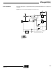
Figure 78. Port C Schematic Diagram (Pins PC7)
Port D Port D is an 8 bit bi-directional I/O port with optional internal pull-up resistors.
Three I/O memory address locations are allocated for Port D, one each for the Data
Register – PORTD, $12($32), Data Direction Register – DDRD, $11($31) and the Port D
Input Pins
– PIND, $10($30). The Port D Input Pins address is read only, while the Data
Register and the Data Direction Register are read/write.
The Port D output buffers can sink 20 mA. As inputs, Port D pins that are externally
pulled low will source current if the pull-up resistors are activated. Some Port D pins
have alternate functions as shown in Table 53.
PUD
0
1
WP:
WD:
RL:
RP:
RD:
PUD:
WRITE PORTC
WRITE DDRC
READ PORTC LATCH
READ PORTC PIN
READ DDRC
PULL-UP DISABLE
AS2: ASYNCH SELECT T/C2
Table 53. Port D Pins Alternate Functions
Port Pin Alternate Function
PD0 RXD (USART Input Pin)
PD1 TXD (USART Output Pin)
PD2 INT0 (External Interrupt 0 Input)
PD3 INT1 (External Interrupt 1 Input)
PD4 OC1B (Timer/Counter1 Output CompareB Match Output)
PD5 OC1A (Timer/Counter1 Output CompareA Match Output)
PD6 ICP (Timer/Counter1 Input Capture Pin)
PD7 OC2 (Timer/Counter2 Output Compare Match Output)