
Datasheet


144
ATmega323(L)
1457E–11/01
Alternate Functions of Port C • TOSC2 - Port C, Bit 7
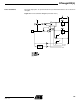
TOSC2, Timer Oscillator pin 2: When the AS2 bit in ASSR is set (one) to enable asyn-
chronous clocking of Timer/Counter2, pin PC7 is disconnected from the port, and
becomes the inverting output of the oscillator amplifier. In this mode, a crystal oscillator
is connected to this pin, and the pin can not be used as an I/O pin.
• TOSC1 - Port C, Bit 6
TOSC1, Timer Oscillator pin 1: When the AS2 bit in ASSR is set (one) to enable asyn-
chronous clocking of Timer/Counter1, pin PC6 is disconnected from the port, and
becomes the input of the inverting oscillator amplifier. In this mode, a crystal oscillator is
connected to this pin, and the pin can not be used as an I/O pin.
• TDI - Port C, Bit 5
TDI, JTAG Test Data In: Serial input data to be shifted in to the Instruction Register or
Data Register (scan chains). When the JTAG interface is enabled, this pin can not be
used as an I/O pin. Refer to the section “JTAG Interface and the On-chip Debug Sys-
tem” on page 153 for details on operation of the JTAG interface.
• TDO - Port C, Bit 4
TDO, JTAG Test Data Out: Serial output data from Instruction register or Data Register.
When the JTAG interface is enabled, this pin can not be used as an I/O pin. Refer to the
section “JTAG Interface and the On-chip Debug System” on page 153 for details on
operation of the JTAG interface.
• TMS - Port C, Bit 3
TMS, JTAG Test Mode Select: This pin is used for navigating through the TAP-controller
state machine. When the JTAG interface is enabled, this pin can not be used as an I/O
pin. Refer to the section “JTAG Interface and the On-chip Debug System” on page 153
for details on operation of the JTAG interface.
• TCK - Port C, Bit 2
TCK, JTAG Test Clock: JTAG operation is synchronous to TCK. When the JTAG inter-
face is enabled, this pin can not be used as an I/O pin. Refer to the section “JTAG
Interface and the On-chip Debug System” on page 153 for details on operation of the
JTAG interface.
• SDA - Port C, Bit 1
SDA, 2-wire Serial Interface Data: When the TWEN bit in TWCR is set (one) to enable
the 2-wire Serial Interface, pin PC1 is disconnected from the port and becomes the
Serial Data I/O pin for the 2-wire Serial Interface. In this mode, there is a spike filter on
the pin to capture spikes shorter than 50 ns on the input signal, and the pin is driven by
an open collector driver with slew rate limitation.
• SCL - Port C, Bit 0
SCL, 2-wire Serial Interface Clock: When the TWEN bit in TWCR is set (one) to enable
the 2-wire Serial Interface, pin PC1 is disconnected from the port and becomes the
Serial Clock I/O pin for the 2-wire Serial Interface. In this mode, there is a spike filter on
the pin to capture spikes shorter than 50 ns on the input signal.