
Datasheet


110
2466T–AVR–07/10
ATmega16(L)
16-bit
Timer/Counter
Register
Description
Timer/Counter1
Control Register A –
TCCR1A
• Bit 7:6 – COM1A1:0: Compare Output Mode for Channel A
• Bit 5:4 – COM1B1:0: Compare Output Mode for Channel B
The COM1A1:0 and COM1B1:0 control the Output Compare pins (OC1A and OC1B respec-
tively) behavior. If one or both of the COM1A1:0 bits are written to one, the OC1A output
overrides the normal port functionality of the I/O pin it is connected to. If one or both of the
COM1B1:0 bit are written to one, the OC1B output overrides the normal port functionality of the
I/O pin it is connected to. However, note that the Data Direction Register (DDR) bit correspond-
ing to the OC1A or OC1B pin must be set in order to enable the output driver.
When the OC1A or OC1B is connected to the pin, the function of the COM1x1:0 bits is depen-
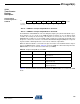
dent of the WGM13:0 bits setting. Table 44 shows the COM1x1:0 bit functionality when the
WGM13:0 bits are set to a normal or a CTC mode (non-PWM).
Table 45 shows the COM1x1:0 bit functionality when the WGM13:0 bits are set to the fast PWM
mode.
Bit 76543210
COM1A1 COM1A0 COM1B1 COM1B0 FOC1A FOC1B WGM11 WGM10 TCCR1A
Read/Write R/W R/W R/W R/W W W R/W R/W
Initial Value00000000
Table 44. Compare Output Mode, non-PWM
COM1A1/COM1B1 COM1A0/COM1B0 Description
0 0 Normal port operation, OC1A/OC1B
disconnected.
0 1 Toggle OC1A/OC1B on compare match
1 0 Clear OC1A/OC1B on compare match (Set
output to low level)
1 1 Set OC1A/OC1B on compare match (Set
output to high level)