
Datasheet


517
AT32UC3A
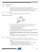
Figure 30-18. Example of an IN Endpoint with 2 Data Banks
30.7.2.12.2 Detailed Description
The data is written by the firmware, following the next flow:
•when the bank is empty, TXINI and FIFOCON are set, what triggers an EPXINT interrupt if
TXINE = 1;
•the firmware acknowledges the interrupt by clearing TXINI;
•the firmware writes the data into the current bank by using the USB Pipe/Endpoint X FIFO
Data register (USB_FIFOX_DATA), until all the data frame is written or the bank is full (in
which case RWALL is cleared by hardware and BYCT reaches the endpoint size);
•the firmware allows the controller to send the bank and switches to the next bank (if any) by
clearing FIFOCON.
If the endpoint uses several banks, the current one can be written by the firmware while the pre-
vious one is being read by the host. Then, when the firmware clears FIFOCON, the following
bank may already be free and TXINI is set immediately.
An “Abort” stage can be produced when a zero-length OUT packet is received during an IN
stage of a control or isochronous IN transaction. The KILLBK bit is used to kill the last written
bank. The best way to manage this abort is to apply the algorithm represented on Figure 30-19.
IN
DATA
(bank 0)
ACK
TXINI
FIFOCON
write data to CPU
BANK 0
SW
SW SW
SW
IN
DATA
(bank 1)
ACK
write data to CPU
BANK 1
SW
HW
write data to CPU
BANK0
32058K
AVR32-01/12