AVR Butterfly Evaluation Kit ..............................................................................................
Table of Contents Section 1 Introduction ........................................................................................... 1-5 1.1 Resources Available on the AVR Butterfly Kit ..........................................1-6 Section 2 How to Operate the Pre-programmed Application................................ 1-7 2.1 2.2 2.3 2.4 Included Firmware ....................................................................................1-7 Joystick Input ...............................................
-iv 4271C–AVR–04/05 AVR Butterfly User Guide
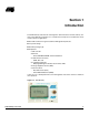
Section 1 Introduction The AVR Butterfly evaluation kit is designed to demonstrate the benefits and key features of the AVR microcontrollers.
1.1 Resources The following resources are available on the Butterfly kit. Available on the ! ATmega169 (MLF-package) AVR Butterfly Kit ! LCD-on-glass display with 120 segments, for demonstrating the ATmega169 LCD controller.
Section 2 How to Operate the Pre-programmed Application The AVR Butterfly comes with a preprogrammed application. This section will go through the basics of this application. The firmware can be downloaded from the AVR Butterfly web-site, http://www.atmel.com/products/AVR/butterfly. 2.
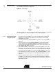
2.2 Joystick Input To operate the AVR Butterfly a joystick is used as user input. It operates in five directions, including center-push, see Figure 2-1. Figure 2-1. Joystick Input Using the joystick one can move around in the menu shown in Figure 2-2, and edit values, entering name, etc. Here are examples on how to enter your name. 2.2.1 Entering Your Name Using the Joystick: 1. Press the joystick up (“SCROLL UP”) to wake the AVR Butterfly.
2.2.2 Entering Your Name Using a Terminal: 1. Connect a serial cable from the PC to the AVR Butterfly as described in Section 3.7 “Connect to PC”, Open a terminal on your PC (e.g. HyperTerminal) and configure the terminal to 19200 Baudrate, 8 Databits, none Parity and one stop bit. 2. Go through point 1, 2 and 3 above. 3. When the “ENTER NAME” is displayed press the joystick down (“SCROLL DOWN”), and “DOWNLOAD NAME” will be displayed 4.
Figure 2-2.
Figure 2-2 shows the menu system of the application that comes with the AVR Butterfly. The column to the left displays the main menu: “AVR Butterfly”, “Time”, “Music” etc… To shift between the alternatives in the menu, press the joystick UP or DOWN. To enter a sub-menu, press the joystick to the RIGHT. To exit a sub-menu, press the joystick to the LEFT. To enter/adjust a value, press ENTER. E.g. when “Adjust clock” appears in the LCD, press ENTER to enter the adjust function. 2.
Figure 2-4. AVR Prog 2.4.2 Jump to the Application Sector From the Boot Section a jump to the application is done by pressing the joystick in the UP-position. 2.4.
Fuse Low Byte (0xE2) – SUT0 (65 ms Start-up Time) – CKSEL3 (Internal RC Oscillator) – CKSEL2 – CKSEL0 Lock Bit Byte (0xEF) – BLB11 (SPM is not allowed to write to the Boot Loader section) Note: AVR Butterfly User Guide For all fuses and lock bits, “1” means unprogrammed and “0” means programmed.
-14 4271C–AVR–04/05 AVR Butterfly User Guide
Section 3 Using the AVR Butterfly This section describes in detail how to use the AVR Butterfly evaluation kit. 3.1 Connectors Some of the I/O-pins on the ATmega169 are available on the connectors of the AVR Butterfly. These connectors are for communication, programming and input to the ADC of the ATmega169. Figure 3-1. Connectors 3.
Figure 3-2. In-System Programming To program the ATmega169 using ISP Programming mode, connect a 6-wire cable between the ISP6PIN connector on the STK500 board and J403 the ISP connector on the AVR Butterfly as shown in Figure 3-2. This device can be programmed using the Serial Programming mode in the AVR Studio4 STK500 software. Instead of soldering in a ISP-header, one can make contact just by pressing the header to the footprint. Make sure that pin 1 on the STK500 match with pin 1 on the AVR Butterfly.
3.2.2 High-voltage Parallel Programming It is possible to program the ATmega169 through the High-voltage Parallel Programming interface. However this requires to move two resistors on the PCB. High-voltage Parallel Programming is only meant to be used in the worst case scenario, where both SPI and the JTAG interface are disabled. To make the parallel programming work, R203 must be placed where the R204 should be, and R404 must be placed where the R403 should be according to Figure 3-4.
Figure 3-6. PORTB and PORTD See the Schematic and the Assembly Drawing in the 7 Complete Schematics for further details. The device can now be programmed using the High-voltage Programming mode in AVR Studio STK500 software. During programming there will be some noise from the piezo element, and some flickering on the LCD, this because PORTB and PORTD are connected to theses modules. Figure 3-7 shows the pinout for the I/O port headers PORT B and PORT D. Figure 3-7.
Note: 3.3 JTAG More information about the STK500 can be found in the STK500 User Guide, which is available at the Atmel web site, www.atmel.com. See the STK500 User Guide for information on how to use the STK500 front-end software in High-voltage Programming mode. Figure 3-8 shows how to connect the JTAG ICE probe to the AVR Butterfly. Figure 3-8. JTAG connector Note: The JTAG connector must be mounted on the back-side of the AVR Butterfly.
Make sure to disable the OCD-fuse after a debugging session, due to power consumption. The OCD-fuse will be disabled if pressing on the “Stop Debugging” button in AvrStudio4, before disconnecting the JTAG ICE probe from the AVR Butterfly. Figure 3-10. External Power External power can be applied at pin 9 and 10 at both PORTB and PORTD, see Figure 3-7 for the pinout. If the JTAG are not in use, the four JTAG pins can be used as input for the ADC channels ADC[4:7].
Figure 3-11. Joystick Schematic 3.6 Sensors The AVR Butterfly has two on-board sensors which makes it possible to measure both temperature and light. In addition is has a voltage-divider that is used to measure voltages from 0 to 5V. 3.6.1 Temperature Sensor The temperature sensor can be found at the back side of the AVR Butterfly. See Figure 3-12.
Figure 3-12. Temperature Sensor An NTC (Negative Temperature Coefficient)-thermistor is used to measure the temperature. An NTC-thermistor is characterised by the fact that when the temperature goes down the resistance goes up. Using a voltage divider and reading the voltage over the thermistor through the ADC-channels on the ATmega169, the temperature in can be calculated. Equation for calculating the temperature in Celsius is shown in Figure 3-13. Figure 3-13.
3.6.2 Light Sensor The light sensor is located at the front of the AVR Butterfly, over the LCD. See Figure 3-15. Figure 3-15. Light Sensor An LDR (Light Dependent Resistor) is used to measure the light. An LDR is characterised by the fact that when the light decreases the resistance goes up. Using a voltage divider and reading the voltage over the LDR through the ADC-channels on the ATmega169, the light can be calculated. 3.6.
Table 3-1. UART AVR Butterfly UART COM2 Pin 1 (RXD) Pin 3 Pin 2 (TXD) Pin 2 Pin 3 (GND) Pin 5 Figure 3-17. UART Connector 3.8 USI The AVR Butterfly has connections for the USI-interface. Figure 3-18 shows the pin-out for the USI. Through the USI interface other modules can be connected, and the AVR Butterfly can serve as a top-module card. Figure 3-18.
Table 3-2. USI AVR Butterfly USI Pin 1 (USCK/SCL) Pin 2 (DI/SDA) Pin 3 (DO) Pin 4 (GND) 3.9 External DataFlash An external dataflash is provided with the AVR Butterfly. This is the 4-megabit serial DataFlash from Atmel, type AT45DB041B. More information about the DataFlash can be found in the datasheet available at the Atmel web site: http://www.atmel.com/products/DataFlash/ The DataFlash is connected to the SPI interface.
3.10 Piezo element A piezo element is used to be able to play sounds on the AVR Butterfly. The piezo is connected to PORTB5 on the ATmega169. And using the PWM, one can get the different frequencies required to play tunes. Figure 3-21. Piezo Element 3.11 Battery Model: CR2450 Nominal Voltage: 3.0 Volts Nominal Capacity: 550 mAh (@0.2 mA Discharge Current, +23ºC) Standard Discharge Current 0.
Section 4 Troubleshooting Guide Table 4-1. Troubleshooting Guide Problem Reason Solution The LCD is not enabled in the AVR device. Check the LCD initialization. (1) The update frequency is not correct. Verify that the clock prescaling correspond with the clock-source.
-28 4271C–AVR–04/05 AVR Butterfly User Guide
Section 5 Technical Specifications System Unit Physical Dimension ………………………………................................…45 x 67 x 14 mm Weight...………………………………………………………………..............................28 g Operation Conditions Temperature…………………………………………………..........................…...0ºC - 50ºC If using external power……………………………………...........................……3,1V - 4,5V Temperature measurement accuracy……………………………….......................…..±1ºC Voltage reading accuracy…………………………………………..........................….
-30 4271C–AVR–04/05 AVR Butterfly User Guide
Section 6 Technical Support For Technical support, please contact avr@atmel.com. When requesting technical support, please include the following information: ! Which target AVR device is used (complete part number) ! Target voltage and speed ! Clock source and fuse setting of the AVR ! Programming method ! Hardware revisions of the AVR tools, found on the PCB ! Version number of AVR Studio (This can be found in the AVR Studio help menu).
-32 4271C–AVR–04/05 AVR Butterfly User Guide
Section 7 Schematics On the following pages the complete schematics and assembly drawing of the AVR Butterfly revision A are shown.
A B C 1 VCP 1 2 GND GND 2 RESET RESET VCC PF0 PF1 GND C106 10N_50V_X7R R100 10K VCC 3 PB7 GND VCC 1 2 3 4 5 6 7 8 9 10 11 12 13 14 15 16 LCDCAP PE0(RXD) PE1(TXD) PE2(AIN0/XCK) PE3(AIN1) PE4(SCL/USCK) PE5(SDA/DI) PE6(DO) PE7 PB0(SS) PB1(SCK) PB2(MOSI) PB3(MISO) PB4(OC0) PB5(OC1A) PB6(OC1B) GND C103 100N_16V_X7R GND LCDCAP PE0 PE1 PE2 PE3 PE4 PE5 PE6 PE7 PB0 PB1 PB2 PB3 PB4 PB5 PB6 2 BLM-21A102S L100 PB[7..0] PB[7..
A B C D 1 R208 100K VCP R205 100K VCC PB[7..0] R206 100K VCC LCD[32..3] 2 1 2 3 4 5 6 7 8 9 10 11 12 13 14 15 16 17 3 4 SO GND VCC WP 8 PB3 7 6 5 V_in D200 BZX399-C1V8 GND R209 300K R212 1M5 AT45DB041B-SC-2.
A B C 1 TXD RXD 2 AVR_RxD AVR_TxD GND GND 0R R302 2 0R R303 2 3 R301 VC080514A300 1 R300 VC080514A300 1 3 BC847BPN Q300A 2 R304 4,7K VCC 2 1 6 1 4 4 1 2 GND 4,7K R305 D300 BAT74 5 5 2 4,7K R306 1 2 1 2 2 3 1 2 1 2 1 4 R307 4,7K 5 6 6 C300 1U_16V_X7R R308 4,7K Q300B BC847BPN VCC 4 3 1 2 4271C–AVR–04/05 1 -36 2 D 1 28-Jan-2003 RS232.Sch 7 TITLE: AVR Butterfly Document number: A0301.3.1000.
A B C 1 PF[7..4] RESET PB[7..0] VCC_EXT 2 PF[7..4] PB[7..
Figure 7-5.
Figure 7-6.
7.1 Bill of Materials Table 7-1.
Table 7-1. Bill Of Material_(Continued) Used Part Type Designator Value Manufacturer Design specific 1 NCP18WF104J03RB R211 100K MURATA * 1 NSL 19M51 R213 SILONEX * 1 PH_2,54_2 X 1 J407 SCOTT ELECT. NOT MOUNTED 1 PH_2,54_3 X 1 J406 SCOTT ELECT. NOT MOUNTED 1 PH_2,54_4 X 1 J405 SCOTT ELECT. NOT MOUNTED 3 PH_2,54_5 X 2 J400 J401 SCOTT ELECT.
Atmel Corporation 2325 Orchard Parkway San Jose, CA 95131, USA Tel: 1(408) 441-0311 Fax: 1(408) 487-2600 Regional Headquarters Europe Atmel Sarl Route des Arsenaux 41 Case Postale 80 CH-1705 Fribourg Switzerland Tel: (41) 26-426-5555 Fax: (41) 26-426-5500 Asia Room 1219 Chinachem Golden Plaza 77 Mody Road Tsimshatsui East Kowloon Hong Kong Tel: (852) 2721-9778 Fax: (852) 2722-1369 Japan 9F, Tonetsu Shinkawa Bldg.