
User manual

4-24 SAM9N12/CN11-EK User Guide
11186A–ATARM–29-Nov-12
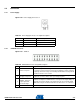
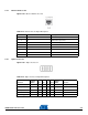
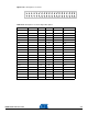
4.4.3 DBGU
Figure 4-30. DBGU Connector J11
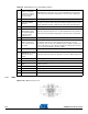
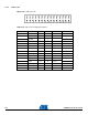
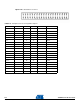
5
TDI TEST DATA
INPUT - Serial data
output line, sampled
on the rising edge of
the TCK signal.
JTAG data input of target CPU. It is recommended that this pin is pulled to a
defined state on the target board. Typically connected to TDI on target CPU.
6 GND Common ground.
7
TMS TEST MODE
SELECT
JTAG mode set input of target CPU. This pin should be pulled up on the target.
Typically connected to TMS on target CPU. Output signal that sequences the
target's JTAG state machine, sampled on the rising edge of the TCK signal.
8 GND Common ground.
9
TCK TEST CLOCK -
Output timing signal,
for synchronizing test
logic and control
register access.
JTAG clock signal to target CPU. It is recommended that this pin is pulled to a
defined state on the target board. Typically connected to TCK on target CPU.
10 GND Common ground.
11
RTCK - Input return
test clock signal from
the target.
Some targets must synchronize the JTAG inputs to internal clocks. To assist in
meeting this requirement, a returned and retimed TCK can be used to
dynamically control the TCK rate. SAM-ICE supports adaptive clocking which
waits for TCK changes to be echoed correctly before making further changes.
Connect to RTCK if available, otherwise to GND.
12 GND Common ground.
13
TDO JTAG TEST
DATA OUTPUT - Serial
data input from the
target.
JTAG data output from target CPU. Typically connected to TDO on target CPU.
14 GND Common ground.
15 nSRST RESET Active-low reset signal. Target CPU reset signal.
16 GND Common ground.
17 RFU This pin is not connected in SAM-ICE.
18 GND Common ground
19 RFU This pin is not connected in SAM-ICE
20 GND Common ground
Table 4-8. JTAG/ICE Connector J4 Signal Descriptions