
User manual


4-10 SAM9N12/CN11-EK User Guide
11186A–ATARM–29-Nov-12
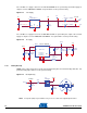
A 3-state buffer is in serial with NAND flash’s CE signal, with PB1 to give a manually disable manner for
NAND boot.
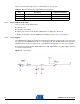
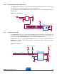
4.3.8 UART DBGU
The Universal Asynchronous Receiver Transmitter features a two-pin UART that can be used for com-
munication and trace purposes and offers an ideal medium for in-situ programming solutions.
This two-pin UART (TXD and RXD only) is buffered through an RS232 transceiver MN16 and brought to
the
DB9 male connector J11.
Figure 4-11. UART
4.
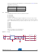
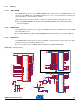
3.9 JTAG Interface
The SAM9N12/CN11-EK board includes a JTAG interface port (J4), to provide debug level access to the
pr
ocessor. The JTAG port is a 20-pin male connector. This port provides the required interface for in-cir-
cuit emulators such as ARM’s Multi-ICE.
Figure 4-12. JTAG
VD DI OP 0
R136
100K
R135
100K
C91
100nF
C94
100nF
MN 16
MA X323 2CSE
T1 IN
11
T2 IN
10
R1OUT
12
R2OUT
9
T1 OU T
14
T2 OU T
7
R1IN
13
R2IN
8
V+
2
C1+
1
C1-
3
C2+
4
C2-
5
V-
6
VCC
16
GND
15
C92
100 nF
C93
100nF
C90
100nF
J11
5
4
3
2
1
9
8
7
6
10
11
PA10
(D TXD)
UART
PA9
(DRXD)
VDD I OP0