
User manual


4-6 SAM9N12/CN11-EK User Guide
11186A–ATARM–29-Nov-12
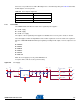
Table 4-1 lists the main components associated with these clock systems.
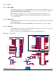
4.3.3 Reset and Wake-up Circuitry
The reset sources for the EK board are:
Power-on reset
Push-button reset (PB2)
JTAG reset from an in-circuit emulator (JTAG interface is equipped on EK board)
To disable any bootable content in NAND Fl
ash or DataFlash, please refer to “Push Buttons” .
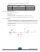
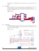
4.3.4 Power Supplies
The SAM9N12/CN11-EK board evaluation and development platform embeds all the necessary power
ra
ils re
quired for the SAM9N12/CN11 processor and peripherals. The SAM9N12/CN11-EK board can be
supplied by either a USB connection via J3 or a 5V DC block through input J1 (refer to usb schematic).
A manual power supply selection (SW1) between the USB supply a
nd the 5V power supply is provided
to select the main power line.
Figure 4-5. Power Input
Tabl
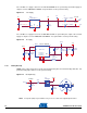
e 4-1. Main Components Associated with the Clock Systems
QTY Description Component assignment
1 Crystal for Internal Clock, 16 MHz Y1
1 Crystal for RTC Clock, 32.768 kHz Y2
1 Crystal for Ethernet Clock, 25 MHz Y3