SAM9N12/CN11-EK ....................................................................................................................
Section 1 Introduction .................................................................................................................1-1 1.1 SAM9N12/CN11 Evaluation Kit.......................................................................................... 1-1 1.2 User Guide Content ........................................................................................................... 1-1 1.3 References and Applicable Documents ..................................................................
4.3.15 Audio.................................................................................................................. 4-14 4.3.16 SD Card ............................................................................................................. 4-15 4.3.17 ZigBee Interface ................................................................................................ 4-15 4.3.18 Analog Interface ................................................................................................
8.1 Revision History .................................................................................................................
Section 1 Introduction 1.1 SAM9N12/CN11 Evaluation Kit This User Guide introduces the SAM9N12 and SAM9CN11 Evaluation Kits and describes their development and debugging capabilities running on SAM9N12 and SAM9CN11 devices. The Atmel ® SAM9N12/CN11 Evaluation Kit is a fully-featured evaluation platform for the Atmel SAM9N12 and SAM9CN11 microcontrollers. The evaluation kit allows users to extensively evaluate, prototype and create application-specific designs.
Section 2 Kit Contents 2.1 Deliverables The Atmel SAM9N12/CN11 Evaluation Kit contains the following items: Board – One SAM9N12/CN11-EK board – One SAM9N12/CN11-DM board Power supply – Universal input AC/DC power supply with US, Europe and UK plug adapters – One 3V lithium battery type CR1225 Cables – One serial RS232 cable – One micro A/B-type USB cable – One RJ45 crossed cable A Welcome letter Figure 2-1.
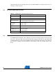
Unpack and inspect the kit carefully. Contact your local Atmel distributor, should you have issues concerning the contents of the kit. 2.2 Evaluation Board Specifications Table 2-1. SAM9N12/CN11 Evaluation Kit Specifications Characteristics 2.
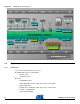
Section 3 Power Up 3.1 Power up the Board Unpack the board, taking care to avoid electrostatic discharge. Unpack the power supply, select the right power plug adapter corresponding to that of your country, and insert it in the power supply. Connect the power supply DC connector to the board and plug the power supply to an AC power plug. The board LCD should light up and display a graphic demo program. Then, click or touch icons displayed on the screen and enjoy the demo. 3.
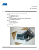
Section 43 Evaluation Kit Hardware 4.1 Board Overview This section introduces the Atmel SAM9N12/CN11 Evaluation Kit design. It introduces system-level concepts, such as power distribution, memory, and interface assignments. The SAM9N12/CN11-EK board is built around on the integration of an ARM®926-based microcontroller (BGA 217 package) with on-board SDRAM, NAND-Flash and a set of popular peripherals.
Figure 4-2. SAM9CN11 Board Architecture 4.2 Equipment List 4.2.1 Features List Here is the list of the EK board components: SAM9N12/CN11 microcontroller BGA – 16 MHz crystal – 32.
– SD/MMC interface Communication – One Ethernet Physical Transceiver Layer with RJ45 connector – UART DBGU port with level shifter IC – JTAG/ICE port – USB Host and Device – ZigBee® Add-on Display Module – TFT LCD module with touch screen – QTouch® elements for user QTouch: K1 to K4 4.2.
Figure 4-3.
Figure 4-4. SAM9CN11-EK Board Layout 4.3 Function Blocks 4.3.1 Processor The EK board is equipped with a SAM9N12/CN11 device in BGA217 package. The processor runs at a nominal frequency of 400 MHz for the core and 133 MHz for the system bus. 4.3.2 Clock Distribution The SAM9N12/CN11-EK board includes three clock systems. Two of the clock systems are alternatives for the SAM9N12/CN11 main clock and one clock system is an oscillator used for the Ethernet controller chip.
Table 4-1 lists the main components associated with these clock systems. Table 4-1. Main Components Associated with the Clock Systems 4.3.3 QTY Description Component assignment 1 Crystal for Internal Clock, 16 MHz Y1 1 Crystal for RTC Clock, 32.
Connector J1 is provided for use with a DC adapter. It is a 2.5 mm male power jack. Table 4-2 below lists the DC adapter connector pinouts. Table 4-2. Power Input Configuration 4.3.5 PIN INPUT 1 (Center) Positive 2 No connection 3 (Outside) Ground Power Rails The SAM9N12/CN11-EK Board contains three regulated power supplies: 3.3V DC supply 1.8V DC supply 1.0V DC core supply The outputs of these regulated power supplies are distributed as necessary to the circuits on boards.
The 1.8V DC core supply is based on an LDO LP38692MP IC. It is powered by the 5V DC supply. Its output is used for VDDIOM and VDDNF. Test point TP6 is used to perform testing. Figure 4-7. 1.8V Supply +5V 4 VIN 3 VOUT L4 TP6 +1V8 1 VDDIOM 220ohm at 100MHz 2 TP7 PWR_EN 1 GND L5 VEN C9 10uF 2 NC VDDNF 220ohm at 100MHz 1 2 TP8 5 C8 4. 7uF MN2 LP38692MP-1.8 The 1.0V DC core supply is based on an LDO ADP1715AR. It is powered by the output of the 3.3V CC supply.
4.3.7 Memory 4.3.7.1 DDR2 SDRAM The SAM9N12/CN11 processor uses DDR2 SDRAM as the system memory. The DDR2 interface uses 1.8V power. The DDR2 chips and SAM9N12/CN11 processor are connected directly. The interface is 1.8V provided by an on-board voltage regulator. VREF, which is half the interface voltage, or 0.9V, is provided by a simple voltage divider of 1.8V. 4.3.7.2 One 1 Gbit DDR2-SDRAM memory (Micron MT47H64M16HR 8Meg*16*8), 16 bits data interface connected to D[0-15].
A 3-state buffer is in serial with NAND flash’s CE signal, with PB1 to give a manually disable manner for NAND boot. 4.3.8 UART DBGU The Universal Asynchronous Receiver Transmitter features a two-pin UART that can be used for communication and trace purposes and offers an ideal medium for in-situ programming solutions. This two-pin UART (TXD and RXD only) is buffered through an RS232 transceiver MN16 and brought to the DB9 male connector J11. Figure 4-11.
4.3.10 Serial Peripheral Interface (SPI) Controller The SAM9N12/CN11 serial processor provides two high-speed Serial Peripheral Interface (SPI) controllers. One port is used to interface with the on-board serial DataFlash. A 3-state buffer is in serial with DataFlash CS signal, with PB1 to give a manually disable manner for DataFlash boot. Figure 4-13.
4.3.12 USB Ports The SAM9N12/CN11-EK features two full speed (OHCI) USB ports: Host full speed, type A USB receptacle, J2 Device full speed, micro B USB receptacle, J3 SAM9N12/CN11-EK features USB power function from device port J3. SW1 functions as switch between USB supply and DC input jack J1. The USB host ports are equipped with 500 mA power switch for bus-powered applications. Figure 4-15.
4.3.13 1-Wire EEPROM The SAM9N12/CN11 Evaluation Kit uses 1-Wire device as “soft label” to store the information such as chip type, manufacture’s name, production date, etc. Figure 4-16. 1-Wire VDDIOP0 R64 1.5K 2 0R 3 4 5 6 NC1 NC2 NC3 NC4 IO 1 R65 GND PA4 MN11 DS2431P+ 4.3.14 ETH on EBI The SAM9N12/CN11 Evaluation Kit uses EBI-based 8-bit EMAC controller KSZ8851 to implement a 10/100 Ethernet access. The board integrates an RJ45 connector with embedded transformer, and two status LEDs.
4.3.15 Audio The SAM9N12/CN11-EK includes a WM8904 audio CODEC for digital sound input and output. This interface includes features and audio jacks for: Line In (J13) Headphone output (J15) Microphone on board The SAM9N12/CN11 programmable clock output PCK0 is used to generate the WM8904 master clock (MCLK). The bit clock is shared; it can be the SSC Transmitter Clock (TK) or the Receiver Clock (RK). The default setting on SAM9N12/CN11-EK is TK and RK shorted together through R159/R160.
4.3.16 SD Card The SAM9N12/CN11 has a high-speed Multimedia Card Interface (MCI). It is used as a 4-bit interface connected to an SD card slot. Figure 4-19.
4.3.18 Analog Interface The 3.0V voltage reference is based on an LM4040 (Precision Micropower Shunt Voltage Reference). This ADVREF level can be set as 3.0V or 3.3V via the jumper JP3. Figure 4-21. Analog Reference A 10 kohm potentiometer (VR1) is connected to AD6 port PB17 to implement an easy access to ADC programming and debugging (or to implement an analog user control such as display brightness, volume, etc). Figure 4-22. Potentiometer 4.3.
4.3.20 Push Buttons SAM9N12/CN11-EK has three mechanical push buttons for system application (PB1 to PB3) and one for free use (PB4). 4.3.20.1 PB1 Output Enable Chip Select Access to the RomBoot: 1. Press simultaneously the PBs OE-CS and NRST 2. Release the PB NRST 3. Then release PB OE-CS The program boots to the ROM code whatever the contents of the NAND Flash or serial DataFlash. Please refer to SAM9N12/CN11 datasheet boot strategy for details. Figure 4-24. PB1 4.3.20.
4.3.21 Expansion Ports Most of GPIOs are led to expansion ports J5, J6, J7. LCD and touch screen connector include J9 and J10 to interface DM board. Figure 4-26.
4.3.22 PIO Usage PIO A Pin Assignment Table 4-3.
PIO B Pin Assignment Table 4-4.
PIO C Pin Assignment Table 4-5.
PIO D Pin Assignment Table 4-6.
4.4 Connectors 4.4.1 Power Supply Figure 4-28. Power Supply Connector J1 Table 4-7. Power Supply Connector J1 Signal Descriptions 4.4.2 Pin Mnemonic 1 Center Signal description +5V 2 Floating 3 GND JTAG/ICE Connector Figure 4-29. JTAG J4 Table 4-8. JTAG/ICE Connector J4 Signal Descriptions Pin Mnemonic Signal Description 1 VTref. 3.3V power This is the target reference voltage.
Table 4-8. JTAG/ICE Connector J4 Signal Descriptions 4.4.3 5 TDI TEST DATA INPUT - Serial data output line, sampled on the rising edge of the TCK signal. JTAG data input of target CPU. It is recommended that this pin is pulled to a defined state on the target board. Typically connected to TDI on target CPU. 6 GND Common ground. 7 TMS TEST MODE SELECT JTAG mode set input of target CPU. This pin should be pulled up on the target. Typically connected to TMS on target CPU.
Table 4-9. DBGU Connector J11 Signal Descriptions Pin Mnemonic PIO (Via translator) 1, 4, 6, 9 No connection 2 RXD (Received Data) PA9 RS232 serial data output signal 3 TXD (Transmitted Data) PA10 RS232 serial data input signal 5 GND Common ground 7 RTS (Request To Send) Not used 8 CTS (Clear To Send) Not used Mechanical pins 4.4.4 Description Shield USB MicroB Figure 4-31. USB Device Micro B Connector J3 Table 4-10. USB Device Micro B Connector J3 Signal Descriptions 4.4.
Table 4-11. USB Type A Port J2 Signal Descriptions 4.4.6 Pin Mnemonic Description 1 Vbus 5V power 2 DM Data minus 3 DP Data plus 4 GND Common ground 5, 6 Shield Mechanical pins SD Card MCI Figure 4-33. SD/MMC Socket J8 Table 4-12.
4.4.7 Ethernet RJ45 Socket Figure 4-34. Ethernet RJ45 Socket J16 Table 4-13. RJ45 Socket J16 Signal Descriptions Pin 4.4.8 Mnemonic Description 1 TX+ Differential output plus 2 TX- Differential output minus 3 RX+ Differential input plus 4 Reserved 5 Reserved 6 RX- 7 Reserved 8 Reserved Differential input minus Zigbee Socket J12 Figure 4-35. Zigbee Socket J12 Table 4-14.
4.4.9 LCD Socket Figure 4-36. LCD Socket J9 Table 4-15.
Figure 4-37. LCD Socket J10 Table 4-16.
4.4.10 IO Expansion Port Figure 4-38. IO Expansion Socket J5 Table 4-17.
Figure 4-39. IO Expansion Socket J6 Table 4-18.
Figure 4-40. IO Expansion Socket J7 Table 4-19.
Section 5 EK Schematics 5.
7 5 4 3 2 1 3V3 POWER SUPPLY EBI DDR2 INTERFACE POWER USER INTERFACE 1V8 1V PIO EBI DATA INTERFACE EBI FLASH INTERFACE Sheet 2,5,7 ICE INTERFACE PIO A,...E Sheet 3 ATMEL ARM9 Processor SAM9N12 (LFBGA217) EBI BUS INTERFACE EBI ETH INTERFACE RS232 C (RJ 45) Sheet 6 PIO 10/100 FAST ETHERNET HOST DEVICE HE 10 EBI NANDFLASH INTERFACE EBI ADDRESS INTERFACE EBI USB HOST NAND FLASH RES.ARRAYS EBI ADAPTER FLASH D EBI D 6 DDR2 128MB 5V 8 C DBGU Sheet 9 Sheet 4 4.
8 7 6 5 4 3 2 1 D D TP1 MN1 RT9018A +5V FORCE POWER ON 3 4 JP1 +5V 1 + C1 10uF 2 C2 1uF 5 VIN VDD VOUT 2 R4 100K EN C7 15pF (3) SHDN 1 PGOOD ADJ C3 100nF R2 47K 1 + C4 10uF 2 5 3 4 R5 10K VDDIOP0 220ohm at 100MHz 2 TP3 L2 C5 1uF 1 7 VDDIOP1 220ohm at 100MHz 2 TP4 L3 VDDANA 220ohm at 100MHz 1 2 8 9 6 GND GND Q1 1 6 R1 100K NC L1 TP2 +3V3 R3 15K TP5 +5V TP9 PWR_EN R6 10K C MN2 LP38692MP-1.
8 7 6 5 4 +3V3 C14 100nF L6 +5V_LCD +5V 220ohm at 100MHz 1 2 TP12 8 OUTA 7 C17 100nF L7 6 220ohm at 100MHz 1 2 TP14 B MN6 + C15 33uF D R15 5 ENA IN FLGA GNG FLGB OUTB ENB 1 R16 0R 2 R17 0R PC31 3 R18 0R PB8 4 R19 0R PB7 47K MN5 SN74LVC1G32 5 1 VCC A 4 Y GND 2 3 2 1 +3V3 LCD_DET (7) PC25 VDDBU 3 D1 BAT54C JP2 +3V3 BT1 1 3 TP13 2 C16 100nF C18 2.
5 4 3 2 1 EBI_D[0..
5 4 3 2 1 JP5 +5V MN7B SAM9N12_LBGA217 - PIOA PA0/TXD0/SPI1_NPCS1 PA1/RXD0/SPI0_NPCS2 PA2/RTS0 PA3/CTS0 PA4/SCK0 PA5/TXD1 PA6/RXD1 PA7/TXD2/SPI0_NPCS1 PA8/RXD2/SPI1_NPCS0 PA9/DRXD PA10/DTXD PA11/SPI0_MISO/MCI_DA4 PA12/SPI0_MOSI/MCI_DA5 PA13/SPI0_SPCK/MCI_DA6 PA14/SPI0_NPCS0/MCI_DA7 PA15/MCI_DA0 PA16/MCI_CDA PA17/MCI_CK PA18/MCI_DA1 PA19/MCI_DA2 PA20/MCI_DA3 PA21/TIOA0/SPI1_MISO PA22/TIOA1/SPI1_MOSI PA23/TIOA2/SPI1_SPCK PA24/TCLK0/TK PA25/TCLK1/TF PA26/TCLK2/TD PA27/TIOB0/RD PA28/TIOB1/RK PA29/TIOB2/RF
5 4 3 2 1 (4) FLASH_D[0..15] (4) FLASH_A[1..23] MN13 (4) DDR2_D[0..15] D (4) DDR2_A[2..
8 7 6 5 4 3 2 1 PA[0..
5 4 3 2 1 L14 (3,5,7) PB[0..18] AUD_1V8 PB10 AVDD1V8 1 D (5,7) PA[0..31] PA24 PA25 PA26 PA27 PA28 PA29 PA30 PA31 AUD_1V8 + C100 10uF C99 100nF C101 100nF 220ohm at 100MHz 2 D R192 0R R193 0R 2 3 AGND_AUDIO J13 4 +3V3 C106 10uF C107 100nF C108 4.7uF C102 100nF C103 100nF R154 20R R155 20R R152 3.9K R153 3.
5 4 3 2 1 L22 +1V8 D 1 C126 10uF C127 100nF C128 100nF C129 100nF A1V8 220ohm at 100MHz 2 C130 100nF C131 100nF D C132 4.7uF GND_ETH GND_ETH L23 A3V3 1 C133 100nF A1V8 +3V3 220ohm at 100MHz 2 C134 10uF +1V8 +1V8 R180 DNP R181 47K R182 47K (4) A1 (4,5) (4,6) (4,6) (4,5) PD19 NWRE NRD PD21 (4,5) PD20 12 6 5 4 R187 3 22R 21 J16 J00-0061 1 TD+ TXP1 TXM1 RXP1 RXM1 3 A GND Y 1 TX- 2 3 RD+ 17 5 CT R176 R177 EECS EESK EED_IO 49.9R 1% R183 DNP 15 10 9 R178 49.
5.
7 5 4 3 2 1 3V3 POWER SUPPLY EBI DDR2 INTERFACE POWER USER INTERFACE 1V8 EBI DATA INTERFACE EBI FLASH INTERFACE Sheet 2,5,7 Sheet 6 ATMEL ARM9 Processor SAM9CN11 (LFBGA217) ICE INTERFACE PIO A,...E Sheet 3 EBI BUS INTERFACE EBI ETH INTERFACE RS232 C (RJ 45) PIO 10/100 FAST ETHERNET HOST DEVICE HE 10 EBI NANDFLASH INTERFACE EBI ADDRESS INTERFACE EBI USB HOST NAND FLASH RES.ARRAYS EBI ADAPTER FLASH D 1V PIO EBI D 6 DDR2 128MB 5V 8 C DBGU Sheet 9 Sheet 4 4.
8 7 6 5 4 3 2 1 D D TP1 MN1 RT9018A +5V FORCE POWER ON 3 4 JP1 +5V 1 + C1 10uF 2 C2 1uF 5 VIN VDD VOUT 6 EN C7 15pF (3) SHDN 1 PGOOD ADJ C3 100nF R2 47K 1 + C4 10uF 2 5 3 4 R5 10K VDDIOP0 220ohm at 100MHz 2 TP3 L2 C5 1uF 1 7 VDDIOP1 220ohm at 100MHz 2 TP4 L3 8 9 1 2 GND GND Q1 R4 100K 6 R1 100K NC L1 TP2 +3V3 1 R3 15K VDDANA 220ohm at 100MHz 2 TP5 +5V TP9 PWR_EN R6 10K C MN2 LP38692MP-1.
8 7 6 5 4 +3V3 C14 100nF L6 +5V_LCD +5V 220ohm at 100MHz 1 2 TP12 8 OUTA 7 C17 100nF L7 6 220ohm at 100MHz 1 2 TP14 B MN6 + C15 33uF D R15 5 ENA IN FLGA GNG FLGB OUTB ENB 1 R16 0R 2 R17 0R PC31 3 R18 0R PB8 4 R19 0R PB7 47K MN5 SN74LVC1G32 5 1 VCC A 4 Y GND 2 3 2 1 +3V3 LCD_DET (7) PC25 VDDBU 3 D1 BAT54C JP2 +3V3 BT1 1 3 TP13 2 C16 100nF C18 2.
5 4 3 2 1 EBI_D[0..
5 4 3 2 1 JP5 +5V PA0/TXD0/SPI1_NPCS1 PA1/RXD0/SPI0_NPCS2 PA2/RTS0 PA3/CTS0 PA4/SCK0 PA5/TXD1 PA6/RXD1 PA7/TXD2/SPI0_NPCS1 PA8/RXD2/SPI1_NPCS0 PA9/DRXD PA10/DTXD PA11/SPI0_MISO/MCI_DA4 PA12/SPI0_MOSI/MCI_DA5 PA13/SPI0_SPCK/MCI_DA6 PA14/SPI0_NPCS0/MCI_DA7 PA15/MCI_DA0 PA16/MCI_CDA PA17/MCI_CK PA18/MCI_DA1 PA19/MCI_DA2 PA20/MCI_DA3 PA21/TIOA0/SPI1_MISO PA22/TIOA1/SPI1_MOSI PA23/TIOA2/SPI1_SPCK PA24/TCLK0/TK PA25/TCLK1/TF PA26/TCLK2/TD PA27/TIOB0/RD PA28/TIOB1/RK PA29/TIOB2/RF PA30/TWD0/SPI1_NPCS3 PA31/
5 4 3 2 1 (4) FLASH_D[0..15] (4) FLASH_A[1..23] MN13 (4) DDR2_D[0..15] (4) DDR2_A[2..
8 7 6 5 4 3 2 1 PA[0..
5 4 3 2 1 L14 (3,5,7) PB[0..18] AUD_1V8 PB10 AVDD1V8 1 (5,7) PA[0..31] PA24 PA25 PA26 PA27 PA28 PA29 PA30 PA31 AUD_1V8 + C100 10uF C99 100nF C101 100nF D 220ohm at 100MHz 2 D R192 0R R193 0R 2 3 AGND_AUDIO J13 4 +3V3 C106 10uF C107 100nF C108 4.7uF C102 100nF C103 100nF R154 20R R155 20R R152 3.9K R153 3.
5 4 3 2 1 L22 +1V8 D 1 C126 10uF C127 100nF C128 100nF C129 100nF A1V8 220ohm at 100MHz 2 C130 100nF C131 100nF D C132 4.7uF GND_ETH GND_ETH L23 A3V3 1 C133 100nF A1V8 220ohm at 100MHz 2 +3V3 C134 10uF +1V8 +1V8 R180 DNP R181 47K R182 47K (4,5) (4,6) (4,6) (4,5) (4,5) 11 A1 12 6 5 4 PD19 NWRE NRD PD21 PD20 R187 3 22R 21 J16 J00-0061 1 TD+ TXP1 TXM1 RXM1 NRST 2 3 A GND Y 16 3 RD+ RX+ 3 17 5 CT RX- 6 R176 R177 EECS EESK EED_IO 15 10 9 R178 49.
Section 6 Display Module Hardware 6.1 Board Overview SAM9N12/CN11-DM board carries a 4.3” TFT LCD module with touch screen. The DM board also carries four QTouch pads. Figure 6-1. 6.2 DM Board Equipment List Here is the list of the DM board components: One 4.3” TFT LCD module LCD Back light driver 3.
6.3 Function Blocks 6.3.1 3.3V Regulator The SAM9N12/CN11-DM board features its own LDO for local power regulation. It accepts DC 5V power from a 500 mA power switch on the EK and outputs a regulated +3.3V to most other circuits on the board. Figure 6-2. DM Board Power Supply 5V_INTER 3V3_LCD MN3 1 5 VIN 2 6.3.2 GND 3 SELCONF IG C12 10u VOUT 4 EN C13 100n C15 2.
LCD with Touch Panel J1 M1 DGMD 41 Figure 6-3. C ond ucto rs on TOP SIDE PIN 40 4.
6.3.4 QTouch The SAM9N12/CN11-DM board carries a QTouch device piloted through a TWI interface. It manages four capacitive touch buttons directly printed on the PCB. There are dual footprints for the QTouch device, and SOIC is the default mounted one. Figure 6-5. QTouch 3V3_LCD MN5 C22 3V3_LCD 3V3_LCD C21 R75 R67 R70 R73 DNPDNP 9 100n 6.3.5 VSS KEY0 KEY1 KEY2 KEY3 KEY4 KEY5 14 13 12 11 10 9 8 R65 R66 R68 R69 4.7k 4.7k 4.7k 4.
Section 7 DM Schematics 7.
5 4 3 2 3V3_LCD 41 R5 R6 DGMD J1 M1 D Conductors on TOP SIDE PIN 40 4.
Section 8 Revision History 8.1 Revision History Table 8-1. Document Comments 11186A First issue. SAM9N12/CN11-EK User Guide Change Request Ref.
Headquarters International Atmel Corporation 2325 Orchard Parkway San Jose, CA 95131 USA Tel: (+1) (408) 441-0311 Fax: (+1) (408) 487-2600 Atmel Asia Limited Unit 01-5 & 16, 19F BEA Tower, Millennium City 5 418 Kwun Tong Road Kwun Tong, Kowloon HONG KONG Tel: (+852) 2245-6100 Fax: (+852) 2722-1369 Atmel Munich GmbH Business Campus Parkring 4 D-85748 Garching b. Munich GERMANY Tel: (+49) 89-31970-0 Fax: (+49) 89-3194621 Atmel Japan 9F, Tonetsu Shinkawa Bldg.