
Datasheet


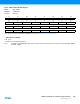
Table Of Contents
- Description
- 1. Features
- 2. Block Diagram
- 3. Signal Description
- 4. Package and Pinout
- 5. Power Considerations
- 6. Memories
- 7. System Controller
- 8. Peripherals
- 9. ARM926EJ-S Processor Overview
- 9.1 Description
- 9.2 Embedded Characteristics
- 9.3 Block Diagram
- 9.4 ARM9EJ-S Processor
- 9.5 CP15 Coprocessor
- 9.6 Memory Management Unit (MMU)
- 9.7 Caches and Write Buffer
- 9.8 Bus Interface Unit
- 10. Debug and Test
- 11. Advanced Interrupt Controller (AIC)
- 11.1 Description
- 11.2 Embedded Characteristics
- 11.3 Block Diagram
- 11.4 Application Block Diagram
- 11.5 AIC Detailed Block Diagram
- 11.6 I/O Line Description
- 11.7 Product Dependencies
- 11.8 Functional Description
- 11.9 Write Protection Registers
- 11.10 Advanced Interrupt Controller (AIC) User Interface
- 11.10.1 Base Address
- 11.10.2 AIC Source Mode Register
- 11.10.3 AIC Source Vector Register
- 11.10.4 AIC Interrupt Vector Register
- 11.10.5 AIC FIQ Vector Register
- 11.10.6 AIC Interrupt Status Register
- 11.10.7 AIC Interrupt Pending Register
- 11.10.8 AIC Interrupt Mask Register
- 11.10.9 AIC Core Interrupt Status Register
- 11.10.10 AIC Interrupt Enable Command Register
- 11.10.11 AIC Interrupt Disable Command Register
- 11.10.12 AIC Interrupt Clear Command Register
- 11.10.13 AIC Interrupt Set Command Register
- 11.10.14 AIC End of Interrupt Command Register
- 11.10.15 AIC Spurious Interrupt Vector Register
- 11.10.16 AIC Debug Control Register
- 11.10.17 AIC Fast Forcing Enable Register
- 11.10.18 AIC Fast Forcing Disable Register
- 11.10.19 AIC Fast Forcing Status Register
- 11.10.20 AIC Write Protect Mode Register
- 11.10.21 AIC Write Protect Status Register
- 12. Boot Strategies
- 13. Boot Sequence Controller (BSC)
- 14. Reset Controller (RSTC)
- 15. Real-time Clock (RTC)
- 15.1 Description
- 15.2 Embedded Characteristics
- 15.3 Block Diagram
- 15.4 Product Dependencies
- 15.5 Functional Description
- 15.6 Real-time Clock (RTC) User Interface
- 15.6.1 RTC Control Register
- 15.6.2 RTC Mode Register
- 15.6.3 RTC Time Register
- 15.6.4 RTC Calendar Register
- 15.6.5 RTC Time Alarm Register
- 15.6.6 RTC Calendar Alarm Register
- 15.6.7 RTC Status Register
- 15.6.8 RTC Status Clear Command Register
- 15.6.9 RTC Interrupt Enable Register
- 15.6.10 RTC Interrupt Disable Register
- 15.6.11 RTC Interrupt Mask Register
- 15.6.12 RTC Valid Entry Register
- 16. Periodic Interval Timer (PIT)
- 17. Watchdog Timer (WDT)
- 18. Shutdown Controller (SHDWC)
- 19. General-Purpose Backup Registers (GPBR)
- 20. Slow Clock Controller (SCKC)
- 21. Clock Generator
- 22. Power Management Controller (PMC)
- 22.1 Description
- 22.2 Embedded Characteristics
- 22.3 Block Diagram
- 22.4 Master Clock Controller
- 22.5 Processor Clock Controller
- 22.6 USB Device and Host Clocks
- 22.7 LP-DDR/DDR2 Clock
- 22.8 Peripheral Clock Controller
- 22.9 Programmable Clock Output Controller
- 22.10 Programming Sequence
- 22.11 Clock Switching Details
- 22.12 Power Management Controller (PMC) User Interface
- 22.12.1 PMC System Clock Enable Register
- 22.12.2 PMC System Clock Disable Register
- 22.12.3 PMC System Clock Status Register
- 22.12.4 PMC Peripheral Clock Enable Register
- 22.12.5 PMC Peripheral Clock Disable Register
- 22.12.6 PMC Peripheral Clock Status Register
- 22.12.7 PMC Clock Generator Main Oscillator Register
- 22.12.8 PMC Clock Generator Main Clock Frequency Register
- 22.12.9 PMC Clock Generator PLLA Register
- 22.12.10 PMC Clock Generator PLLB Register
- 22.12.11 PMC Master Clock Register
- 22.12.12 USB Clock Register
- 22.12.13 PMC Programmable Clock Register
- 22.12.14 PMC Interrupt Enable Register
- 22.12.15 PMC Interrupt Disable Register
- 22.12.16 PMC Status Register
- 22.12.17 PMC Interrupt Mask Register
- 22.12.18 PLL Charge Pump Current Register
- 22.12.19 PMC Write Protect Mode Register
- 22.12.20 PMC Write Protect Status Register
- 22.12.21 PMC Peripheral Control Register
- 23. Parallel Input/Output Controller (PIO)
- 23.1 Description
- 23.2 Embedded Characteristics
- 23.3 Block Diagram
- 23.4 Product Dependencies
- 23.5 Functional Description
- 23.5.1 Pull-up and Pull-down Resistor Control
- 23.5.2 I/O Line or Peripheral Function Selection
- 23.5.3 Peripheral A or B or C or D Selection
- 23.5.4 Output Control
- 23.5.5 Synchronous Data Output
- 23.5.6 Multi-Drive Control (Open Drain)
- 23.5.7 Output Line Timings
- 23.5.8 Inputs
- 23.5.9 Input Glitch and Debouncing Filters
- 23.5.10 Input Edge/Level Interrupt
- 23.5.11 Programmable I/O Delays
- 23.5.12 Programmable I/O Drive
- 23.5.13 Programmable Schmitt Trigger
- 23.5.14 Register Write Protection
- 23.6 I/O Lines Programming Example
- 23.7 Parallel Input/Output Controller (PIO) User Interface
- 23.7.1 PIO Enable Register
- 23.7.2 PIO Disable Register
- 23.7.3 PIO Status Register
- 23.7.4 PIO Output Enable Register
- 23.7.5 PIO Output Disable Register
- 23.7.6 PIO Output Status Register
- 23.7.7 PIO Input Filter Enable Register
- 23.7.8 PIO Input Filter Disable Register
- 23.7.9 PIO Input Filter Status Register
- 23.7.10 PIO Set Output Data Register
- 23.7.11 PIO Clear Output Data Register
- 23.7.12 PIO Output Data Status Register
- 23.7.13 PIO Pin Data Status Register
- 23.7.14 PIO Interrupt Enable Register
- 23.7.15 PIO Interrupt Disable Register
- 23.7.16 PIO Interrupt Mask Register
- 23.7.17 PIO Interrupt Status Register
- 23.7.18 PIO Multi-driver Enable Register
- 23.7.19 PIO Multi-driver Disable Register
- 23.7.20 PIO Multi-driver Status Register
- 23.7.21 PIO Pull-Up Disable Register
- 23.7.22 PIO Pull-Up Enable Register
- 23.7.23 PIO Pull-Up Status Register
- 23.7.24 PIO Peripheral ABCD Select Register 1
- 23.7.25 PIO Peripheral ABCD Select Register 2
- 23.7.26 PIO Input Filter Slow Clock Disable Register
- 23.7.27 PIO Input Filter Slow Clock Enable Register
- 23.7.28 PIO Input Filter Slow Clock Status Register
- 23.7.29 PIO Slow Clock Divider Debouncing Register
- 23.7.30 PIO Pad Pull-Down Disable Register
- 23.7.31 PIO Pad Pull-Down Enable Register
- 23.7.32 PIO Pad Pull-Down Status Register
- 23.7.33 PIO Output Write Enable Register
- 23.7.34 PIO Output Write Disable Register
- 23.7.35 PIO Output Write Status Register
- 23.7.36 PIO Additional Interrupt Modes Enable Register
- 23.7.37 PIO Additional Interrupt Modes Disable Register
- 23.7.38 PIO Additional Interrupt Modes Mask Register
- 23.7.39 PIO Edge Select Register
- 23.7.40 PIO Level Select Register
- 23.7.41 PIO Edge/Level Status Register
- 23.7.42 PIO Falling Edge/Low-Level Select Register
- 23.7.43 PIO Rising Edge/High-Level Select Register
- 23.7.44 PIO Fall/Rise - Low/High Status Register
- 23.7.45 PIO Write Protection Mode Register
- 23.7.46 PIO Write Protection Status Register
- 23.7.47 PIO Schmitt Trigger Register
- 23.7.48 PIO I/O Delay Register
- 23.7.49 PIO I/O Drive Register 1
- 23.7.50 PIO I/O Drive Register 2
- 24. Debug Unit (DBGU)
- 24.1 Description
- 24.2 Embedded Characteristics
- 24.3 Block Diagram
- 24.4 Product Dependencies
- 24.5 UART Operations
- 24.6 Debug Unit (DBGU) User Interface
- 24.6.1 Debug Unit Control Register
- 24.6.2 Debug Unit Mode Register
- 24.6.3 Debug Unit Interrupt Enable Register
- 24.6.4 Debug Unit Interrupt Disable Register
- 24.6.5 Debug Unit Interrupt Mask Register
- 24.6.6 Debug Unit Status Register
- 24.6.7 Debug Unit Receiver Holding Register
- 24.6.8 Debug Unit Transmit Holding Register
- 24.6.9 Debug Unit Baud Rate Generator Register
- 24.6.10 Debug Unit Chip ID Register
- 24.6.11 Debug Unit Chip ID Extension Register
- 24.6.12 Debug Unit Force NTRST Register
- 25. Fuse Controller (FUSE)
- 26. Bus Matrix (MATRIX)
- 26.1 Description
- 26.2 Embedded Characteristics
- 26.3 Matrix Masters
- 26.4 Matrix Slaves
- 26.5 Master to Slave Access
- 26.6 Memory Mapping
- 26.7 Special Bus Granting Mechanism
- 26.8 Arbitration
- 26.9 Write Protect Registers
- 26.10 Bus Matrix (MATRIX) User Interface
- 26.10.1 Bus Matrix Master Configuration Registers
- 26.10.2 Bus Matrix Slave Configuration Registers
- 26.10.3 Bus Matrix Priority Registers A For Slaves
- 26.10.4 Bus Matrix Master Remap Control Register
- 26.10.5 Chip Configuration User Interface
- 26.10.6 Write Protect Mode Register
- 26.10.7 Write Protect Status Register
- 27. External Bus Interface (EBI)
- 27.1 Description
- 27.2 Embedded Characteristics
- 27.3 EBI Block Diagram
- 27.4 I/O Lines Description
- 27.5 Application Example
- 27.6 Product Dependencies
- 27.7 Functional Description
- 27.8 Implementation Examples
- 28. Programmable Multibit ECC Controller (PMECC)
- 28.1 Description
- 28.2 Embedded Characteristics
- 28.3 Block Diagram
- 28.4 Functional Description
- 28.5 Software Implementation
- 28.6 Programmable Multibit ECC Controller (PMECC) User Interface
- 28.6.1 PMECC Configuration Register
- 28.6.2 PMECC Spare Area Size Register
- 28.6.3 PMECC Start Address Register
- 28.6.4 PMECC End Address Register
- 28.6.5 PMECC Clock Control Register
- 28.6.6 PMECC Control Register
- 28.6.7 PMECC Status Register
- 28.6.8 PMECC Interrupt Enable Register
- 28.6.9 PMECC Interrupt Disable Register
- 28.6.10 PMECC Interrupt Mask Register
- 28.6.11 PMECC Interrupt Status Register
- 28.6.12 PMECC ECC x Register
- 28.6.13 PMECC Remainder x Register
- 29. Programmable Multibit ECC Error Location Controller (PMERRLOC)
- 29.1 Description
- 29.2 Embedded Characteristics
- 29.3 Block Diagram
- 29.4 Functional Description
- 29.5 Programmable Multibit ECC Error Location (PMERRLOC) User Interface
- 29.5.1 Error Location Configuration Register
- 29.5.2 Error Location Primitive Register
- 29.5.3 Error Location Enable Register
- 29.5.4 Error Location Disable Register
- 29.5.5 Error Location Status Register
- 29.5.6 Error Location Interrupt Enable Register
- 29.5.7 Error Location Interrupt Disable Register
- 29.5.8 Error Location Interrupt Mask Register
- 29.5.9 Error Location Interrupt Status Register
- 29.5.10 Error Location SIGMAx Register
- 29.5.11 PMECC Error Locationx Register
- 30. Static Memory Controller (SMC)
- 30.1 Description
- 30.2 Embedded Characteristics
- 30.3 I/O Lines Description
- 30.4 Multiplexed Signals
- 30.5 Application Example
- 30.6 Product Dependencies
- 30.7 External Memory Mapping
- 30.8 Connection to External Devices
- 30.9 Standard Read and Write Protocols
- 30.10 Automatic Wait States
- 30.11 Data Float Wait States
- 30.12 External Wait
- 30.13 Slow Clock Mode
- 30.14 Asynchronous Page Mode
- 30.15 Programmable IO Delays
- 30.16 Static Memory Controller (SMC) User Interface
- 31. DDR SDR SDRAM Controller (DDRSDRC)
- 31.1 Description
- 31.2 Embedded Characteristics
- 31.3 DDRSDRC Module Diagram
- 31.4 Initialization Sequence
- 31.5 Functional Description
- 31.6 Software Interface/SDRAM Organization, Address Mapping
- 31.7 DDR SDR SDRAM Controller (DDRSDRC) User Interface
- 31.7.1 DDRSDRC Mode Register
- 31.7.2 DDRSDRC Refresh Timer Register
- 31.7.3 DDRSDRC Configuration Register
- 31.7.4 DDRSDRC Timing Parameter 0 Register
- 31.7.5 DDRSDRC Timing Parameter 1 Register
- 31.7.6 DDRSDRC Timing Parameter 2 Register
- 31.7.7 DDRSDRC Low-power Register
- 31.7.8 DDRSDRC Memory Device Register
- 31.7.9 DDRSDRC DLL Register
- 31.7.10 DDRSDRC High Speed Register
- 31.7.11 DDRSDRC Write Protect Mode Register
- 31.7.12 DDRSDRC Write Protect Status Register
- 32. DMA Controller (DMAC)
- 32.1 Description
- 32.2 Embedded Characteristics
- 32.3 DMA Controller Peripheral Connections
- 32.4 Block Diagram
- 32.5 Functional Description
- 32.6 DMAC Software Requirements
- 32.7 Write Protection Registers
- 32.8 DMA Controller (DMAC) User Interface
- 32.8.1 DMAC Global Configuration Register
- 32.8.2 DMAC Enable Register
- 32.8.3 DMAC Software Single Request Register
- 32.8.4 DMAC Software Chunk Transfer Request Register
- 32.8.5 DMAC Software Last Transfer Flag Register
- 32.8.6 DMAC Error, Buffer Transfer and Chained Buffer Transfer Interrupt Enable Register
- 32.8.7 DMAC Error, Buffer Transfer and Chained Buffer Transfer Interrupt Disable Register
- 32.8.8 DMAC Error, Buffer Transfer and Chained Buffer Transfer Interrupt Mask Register
- 32.8.9 DMAC Error, Buffer Transfer and Chained Buffer Transfer Status Register
- 32.8.10 DMAC Channel Handler Enable Register
- 32.8.11 DMAC Channel Handler Disable Register
- 32.8.12 DMAC Channel Handler Status Register
- 32.8.13 DMAC Channel x [x = 0..7] Source Address Register
- 32.8.14 DMAC Channel x [x = 0..7] Destination Address Register
- 32.8.15 DMAC Channel x [x = 0..7] Descriptor Address Register
- 32.8.16 DMAC Channel x [x = 0..7] Control A Register
- 32.8.17 DMAC Channel x [x = 0..7] Control B Register
- 32.8.18 DMAC Channel x [x = 0..7] Configuration Register
- 32.8.19 DMAC Channel x [x = 0..7] Source Picture-in-Picture Configuration Register
- 32.8.20 DMAC Channel x [x = 0..7] Destination Picture-in-Picture Configuration Register
- 32.8.21 DMAC Write Protect Mode Register
- 32.8.22 DMAC Write Protect Status Register
- 33. USB Device Port (UDP)
- 33.1 Description
- 33.2 Embedded Characteristics
- 33.3 Block Diagram
- 33.4 Product Dependencies
- 33.5 Typical Connection
- 33.6 Functional Description
- 33.7 USB Device Port (UDP) User Interface
- 33.7.1 UDP Frame Number Register
- 33.7.2 UDP Global State Register
- 33.7.3 UDP Function Address Register
- 33.7.4 UDP Interrupt Enable Register
- 33.7.5 UDP Interrupt Disable Register
- 33.7.6 UDP Interrupt Mask Register
- 33.7.7 UDP Interrupt Status Register
- 33.7.8 UDP Interrupt Clear Register
- 33.7.9 UDP Reset Endpoint Register
- 33.7.10 UDP Endpoint Control and Status Register (Control, Bulk Interrupt Endpoints)
- 33.7.11 UDP Endpoint Control and Status Register (Isochronous Endpoints)
- 33.7.12 UDP FIFO Data Register
- 33.7.13 UDP Transceiver Control Register
- 34. USB Host Port (UHP)
- 35. High Speed MultiMedia Card Interface (HSMCI)
- 35.1 Description
- 35.2 Embedded Characteristics
- 35.3 Block Diagram
- 35.4 Application Block Diagram
- 35.5 Pin Name List
- 35.6 Product Dependencies
- 35.7 Bus Topology
- 35.8 High Speed MultiMedia Card Operations
- 35.9 SD/SDIO Card Operation
- 35.10 CE-ATA Operation
- 35.11 HSMCI Boot Operation Mode
- 35.12 HSMCI Transfer Done Timings
- 35.13 Register Write Protection
- 35.14 High Speed MultiMedia Card Interface (HSMCI) User Interface
- 35.14.1 HSMCI Control Register
- 35.14.2 HSMCI Mode Register
- 35.14.3 HSMCI Data Timeout Register
- 35.14.4 HSMCI SDCard/SDIO Register
- 35.14.5 HSMCI Argument Register
- 35.14.6 HSMCI Command Register
- 35.14.7 HSMCI Block Register
- 35.14.8 HSMCI Completion Signal Timeout Register
- 35.14.9 HSMCI Response Register
- 35.14.10 HSMCI Receive Data Register
- 35.14.11 HSMCI Transmit Data Register
- 35.14.12 HSMCI Status Register
- 35.14.13 HSMCI Interrupt Enable Register
- 35.14.14 HSMCI Interrupt Disable Register
- 35.14.15 HSMCI Interrupt Mask Register
- 35.14.16 HSMCI DMA Configuration Register
- 35.14.17 HSMCI Configuration Register
- 35.14.18 HSMCI Write Protection Mode Register
- 35.14.19 HSMCI Write Protection Status Register
- 35.14.20 HSMCI FIFOx Memory Aperture
- 36. Serial Peripheral Interface (SPI)
- 36.1 Description
- 36.2 Embedded Characteristics
- 36.3 Block Diagram
- 36.4 Application Block Diagram
- 36.5 Signal Description
- 36.6 Product Dependencies
- 36.7 Functional Description
- 36.7.1 Modes of Operation
- 36.7.2 Data Transfer
- 36.7.3 Master Mode Operations
- 36.7.3.1 Master Mode Block Diagram
- 36.7.3.2 Master Mode Flow Diagram
- 36.7.3.3 Clock Generation
- 36.7.3.4 Transfer Delays
- 36.7.3.5 Peripheral Selection
- 36.7.3.6 SPI Direct Access Memory Controller (DMAC)
- 36.7.3.7 Peripheral Chip Select Decoding
- 36.7.3.8 Peripheral Deselection without DMA
- 36.7.3.9 Peripheral Deselection with DMAC
- 36.7.3.10 Mode Fault Detection
- 36.7.4 SPI Slave Mode
- 36.7.5 Write Protected Registers
- 36.8 Serial Peripheral Interface (SPI) User Interface
- 36.8.1 SPI Control Register
- 36.8.2 SPI Mode Register
- 36.8.3 SPI Receive Data Register
- 36.8.4 SPI Transmit Data Register
- 36.8.5 SPI Status Register
- 36.8.6 SPI Interrupt Enable Register
- 36.8.7 SPI Interrupt Disable Register
- 36.8.8 SPI Interrupt Mask Register
- 36.8.9 SPI Chip Select Register
- 36.8.10 SPI Write Protection Mode Register
- 36.8.11 SPI Write Protection Status Register
- 37. Timer Counter (TC)
- 37.1 Description
- 37.2 Embedded Characteristics
- 37.3 Block Diagram
- 37.4 Pin Name List
- 37.5 Product Dependencies
- 37.6 Functional Description
- 37.6.1 TC Description
- 37.6.2 32-bit Counter
- 37.6.3 Clock Selection
- 37.6.4 Clock Control
- 37.6.5 TC Operating Modes
- 37.6.6 Trigger
- 37.6.7 Capture Operating Mode
- 37.6.8 Capture Registers A and B
- 37.6.9 Transfer with DMAC
- 37.6.10 Trigger Conditions
- 37.6.11 Waveform Operating Mode
- 37.6.12 Waveform Selection
- 37.6.13 External Event/Trigger Conditions
- 37.6.14 Output Controller
- 37.7 Timer Counter (TC) User Interface
- 37.7.1 TC Channel Control Register
- 37.7.2 TC Channel Mode Register: Capture Mode
- 37.7.3 TC Channel Mode Register: Waveform Mode
- 37.7.4 TC Register AB
- 37.7.5 TC Counter Value Register
- 37.7.6 TC Register A
- 37.7.7 TC Register B
- 37.7.8 TC Register C
- 37.7.9 TC Status Register
- 37.7.10 TC Interrupt Enable Register
- 37.7.11 TC Interrupt Disable Register
- 37.7.12 TC Interrupt Mask Register
- 37.7.13 TC Block Control Register
- 37.7.14 TC Block Mode Register
- 38. Pulse Width Modulation Controller (PWM)
- 38.1 Description
- 38.2 Embedded characteristics
- 38.3 Block Diagram
- 38.4 I/O Lines Description
- 38.5 Product Dependencies
- 38.6 Functional Description
- 38.7 Pulse Width Modulation Controller (PWM) User Interface
- 38.7.1 PWM Mode Register
- 38.7.2 PWM Enable Register
- 38.7.3 PWM Disable Register
- 38.7.4 PWM Status Register
- 38.7.5 PWM Interrupt Enable Register
- 38.7.6 PWM Interrupt Disable Register
- 38.7.7 PWM Interrupt Mask Register
- 38.7.8 PWM Interrupt Status Register
- 38.7.9 PWM Channel Mode Register
- 38.7.10 PWM Channel Duty Cycle Register
- 38.7.11 PWM Channel Period Register
- 38.7.12 PWM Channel Counter Register
- 38.7.13 PWM Channel Update Register
- 39. Two-wire Interface (TWI)
- 39.1 Description
- 39.2 Embedded Characteristics
- 39.3 List of Abbreviations
- 39.4 Block Diagram
- 39.5 Application Block Diagram
- 39.6 Product Dependencies
- 39.7 Functional Description
- 39.8 Master Mode
- 39.9 Multi-master Mode
- 39.10 Slave Mode
- 39.11 Write Protection System
- 39.12 Two-wire Interface (TWI) User Interface
- 39.12.1 TWI Control Register
- 39.12.2 TWI Master Mode Register
- 39.12.3 TWI Slave Mode Register
- 39.12.4 TWI Internal Address Register
- 39.12.5 TWI Clock Waveform Generator Register
- 39.12.6 TWI Status Register
- 39.12.7 TWI Interrupt Enable Register
- 39.12.8 TWI Interrupt Disable Register
- 39.12.9 TWI Interrupt Mask Register
- 39.12.10 TWI Receive Holding Register
- 39.12.11 TWI Transmit Holding Register
- 39.12.12 TWI Write Protection Mode Register
- 39.12.13 TWI Write Protection Status Register
- 40. Universal Synchronous Asynchronous Receiver Transceiver (USART)
- 40.1 Description
- 40.2 Embedded Characteristics
- 40.3 Block Diagram
- 40.4 Application Block Diagram
- 40.5 I/O Lines Description
- 40.6 Product Dependencies
- 40.7 Functional Description
- 40.7.1 Baud Rate Generator
- 40.7.2 Receiver and Transmitter Control
- 40.7.3 Synchronous and Asynchronous Modes
- 40.7.3.1 Transmitter Operations
- 40.7.3.2 Manchester Encoder
- 40.7.3.3 Asynchronous Receiver
- 40.7.3.4 Manchester Decoder
- 40.7.3.5 Radio Interface: Manchester Encoded USART Application
- 40.7.3.6 Synchronous Receiver
- 40.7.3.7 Receiver Operations
- 40.7.3.8 Parity
- 40.7.3.9 Multidrop Mode
- 40.7.3.10 Transmitter Timeguard
- 40.7.3.11 Receiver Time-out
- 40.7.3.12 Framing Error
- 40.7.3.13 Transmit Break
- 40.7.3.14 Receive Break
- 40.7.3.15 Hardware Handshaking
- 40.7.4 ISO7816 Mode
- 40.7.5 IrDA Mode
- 40.7.6 RS485 Mode
- 40.7.7 SPI Mode
- 40.7.8 LIN Mode
- 40.7.8.1 Modes of Operation
- 40.7.8.2 Baud Rate Configuration
- 40.7.8.3 Receiver and Transmitter Control
- 40.7.8.4 Character Transmission
- 40.7.8.5 Character Reception
- 40.7.8.6 Header Transmission (Master Node Configuration)
- 40.7.8.7 Header Reception (Slave Node Configuration)
- 40.7.8.8 Slave Node Synchronization
- 40.7.8.9 Identifier Parity
- 40.7.8.10 Node Action
- 40.7.8.11 Response Data Length
- 40.7.8.12 Checksum
- 40.7.8.13 Frame Slot Mode
- 40.7.8.14 LIN Errors
- 40.7.8.15 LIN Frame Handling
- 40.7.8.16 LIN Frame Handling With the DMAC
- 40.7.8.17 Wake-up Request
- 40.7.8.18 Bus Idle Time-out
- 40.7.9 Test Modes
- 40.7.10 Write Protection Registers
- 40.8 Universal Synchronous Asynchronous Receiver Transmitter (USART) User Interface
- 40.8.1 USART Control Register
- 40.8.2 USART Control Register (SPI_MODE)
- 40.8.3 USART Mode Register
- 40.8.4 USART Mode Register (SPI_MODE)
- 40.8.5 USART Interrupt Enable Register
- 40.8.6 USART Interrupt Enable Register (SPI_MODE)
- 40.8.7 USART Interrupt Enable Register (LIN_MODE)
- 40.8.8 USART Interrupt Disable Register
- 40.8.9 USART Interrupt Disable Register (SPI_MODE)
- 40.8.10 USART Interrupt Disable Register (LIN_MODE)
- 40.8.11 USART Interrupt Mask Register
- 40.8.12 USART Interrupt Mask Register (SPI_MODE)
- 40.8.13 USART Interrupt Mask Register (LIN_MODE)
- 40.8.14 USART Channel Status Register
- 40.8.15 USART Channel Status Register (SPI_MODE)
- 40.8.16 USART Channel Status Register (LIN_MODE)
- 40.8.17 USART Receive Holding Register
- 40.8.18 USART Transmit Holding Register
- 40.8.19 USART Baud Rate Generator Register
- 40.8.20 USART Receiver Time-out Register
- 40.8.21 USART Transmitter Timeguard Register
- 40.8.22 USART FI DI RATIO Register
- 40.8.23 USART Number of Errors Register
- 40.8.24 USART IrDA FILTER Register
- 40.8.25 USART Manchester Configuration Register
- 40.8.26 USART LIN Mode Register
- 40.8.27 USART LIN Identifier Register
- 40.8.28 USART LIN Baud Rate Register
- 40.8.29 USART Write Protect Mode Register
- 40.8.30 USART Write Protect Status Register
- 41. Universal Asynchronous Receiver Transmitter (UART)
- 41.1 Description
- 41.2 Embedded Characteristics
- 41.3 Block Diagram
- 41.4 Product Dependencies
- 41.5 UART Operations
- 41.6 Universal Asynchronous Receiver Transmitter (UART) User Interface
- 41.6.1 UART Control Register
- 41.6.2 UART Mode Register
- 41.6.3 UART Interrupt Enable Register
- 41.6.4 UART Interrupt Disable Register
- 41.6.5 UART Interrupt Mask Register
- 41.6.6 UART Status Register
- 41.6.7 UART Receiver Holding Register
- 41.6.8 UART Transmit Holding Register
- 41.6.9 UART Baud Rate Generator Register
- 42. Analog-to-Digital Converter (ADC)
- 42.1 Description
- 42.2 Embedded Characteristics
- 42.3 Block Diagram
- 42.4 Signal Description
- 42.5 Product Dependencies
- 42.6 Functional Description
- 42.7 Touchscreen
- 42.7.1 Touchscreen Mode
- 42.7.2 4-wire Resistive Touchscreen Principles
- 42.7.3 4-wire Position Measurement Method
- 42.7.4 4-wire Pressure Measurement Method
- 42.7.5 5-wire Resistive Touchscreen Principles
- 42.7.6 5-wire Position Measurement Method
- 42.7.7 Sequence and Noise Filtering
- 42.7.8 Measured Values, Registers and Flags
- 42.7.9 Pen Detect Method
- 42.7.10 Buffer Structure
- 42.7.11 Write Protected Registers
- 42.8 Analog-to-Digital Converter (ADC) User Interface
- 42.8.1 ADC Control Register
- 42.8.2 ADC Mode Register
- 42.8.3 ADC Channel Sequence 1 Register
- 42.8.4 ADC Channel Sequence 2 Register
- 42.8.5 ADC Channel Enable Register
- 42.8.6 ADC Channel Disable Register
- 42.8.7 ADC Channel Status Register
- 42.8.8 ADC Last Converted Data Register
- 42.8.9 ADC Interrupt Enable Register
- 42.8.10 ADC Interrupt Disable Register
- 42.8.11 ADC Interrupt Mask Register
- 42.8.12 ADC Interrupt Status Register
- 42.8.13 ADC Overrun Status Register
- 42.8.14 ADC Extended Mode Register
- 42.8.15 ADC Compare Window Register
- 42.8.16 ADC Channel Data Register
- 42.8.17 ADC Analog Control Register
- 42.8.18 ADC Touchscreen Mode Register
- 42.8.19 ADC Touchscreen X Position Register
- 42.8.20 ADC Touchscreen Y Position Register
- 42.8.21 ADC Touchscreen Pressure Register
- 42.8.22 ADC Trigger Register
- 42.8.23 ADC Write Protect Mode Register
- 42.8.24 ADC Write Protect Status Register
- 43. Synchronous Serial Controller (SSC)
- 43.1 Description
- 43.2 Embedded Characteristics
- 43.3 Block Diagram
- 43.4 Application Block Diagram
- 43.5 Pin Name List
- 43.6 Product Dependencies
- 43.7 Functional Description
- 43.8 SSC Application Examples
- 43.9 Synchronous Serial Controller (SSC) User Interface
- 43.9.1 SSC Control Register
- 43.9.2 SSC Clock Mode Register
- 43.9.3 SSC Receive Clock Mode Register
- 43.9.4 SSC Receive Frame Mode Register
- 43.9.5 SSC Transmit Clock Mode Register
- 43.9.6 SSC Transmit Frame Mode Register
- 43.9.7 SSC Receive Holding Register
- 43.9.8 SSC Transmit Holding Register
- 43.9.9 SSC Receive Synchronization Holding Register
- 43.9.10 SSC Transmit Synchronization Holding Register
- 43.9.11 SSC Receive Compare 0 Register
- 43.9.12 SSC Receive Compare 1 Register
- 43.9.13 SSC Status Register
- 43.9.14 SSC Interrupt Enable Register
- 43.9.15 SSC Interrupt Disable Register
- 43.9.16 SSC Interrupt Mask Register
- 43.9.17 SSC Write Protect Mode Register
- 43.9.18 SSC Write Protect Status Register
- 44. LCD Controller (LCDC)
- 44.1 Description
- 44.2 Embedded Characteristics
- 44.3 Block Diagram
- 44.4 I/O Lines Description
- 44.5 Product Dependencies
- 44.6 Functional Description
- 44.6.1 Timing Engine Configuration
- 44.6.2 DMA Software Operations
- 44.6.3 Display Software Configuration
- 44.6.4 RGB Frame Buffer Memory Bitmap
- 44.6.4.1 1 bpp Through Color Lookup Table
- 44.6.4.2 2 bpp Through Color Lookup Table
- 44.6.4.3 4 bpp Through Color Lookup Table
- 44.6.4.4 8 bpp Through Color Lookup Table
- 44.6.4.5 12 bpp Memory Mapping, RGB 4:4:4
- 44.6.4.6 16 bpp Memory Mapping with Alpha Channel, ARGB 4:4:4:4
- 44.6.4.7 16 bpp Memory Mapping with Alpha Channel, RGBA 4:4:4:4
- 44.6.4.8 16 bpp Memory Mapping with Alpha Channel, RGB 5:6:5
- 44.6.4.9 16 bpp Memory Mapping with Transparency Bit, ARGB 1:5:5:5
- 44.6.4.10 18 bpp Unpacked Memory Mapping with Transparency Bit, RGB 6:6:6
- 44.6.4.11 18 bpp Packed Memory Mapping with Transparency Bit, RGB 6:6:6
- 44.6.4.12 19 bpp Unpacked Memory Mapping with Transparency Bit, RGB 1:6:6:6
- 44.6.4.13 19 bpp Packed Memory Mapping with Transparency Bit, ARGB 1:6:6:6
- 44.6.4.14 24 bpp Unpacked Memory Mapping, RGB 8:8:8
- 44.6.4.15 24 bpp Packed Memory Mapping, RGB 8:8:8
- 44.6.4.16 25 bpp Memory Mapping, ARGB 1:8:8:8
- 44.6.4.17 32 bpp Memory Mapping, ARGB 8:8:8:8
- 44.6.4.18 32 bpp Memory Mapping, RGBA 8:8:8:8
- 44.6.5 Output Timing Generation
- 44.6.6 Output Format
- 44.7 LCD Controller (LCDC) User Interface
- 44.7.1 LCD Controller Configuration Register 0
- 44.7.2 LCD Controller Configuration Register 1
- 44.7.3 LCD Controller Configuration Register 2
- 44.7.4 LCD Controller Configuration Register 3
- 44.7.5 LCD Controller Configuration Register 4
- 44.7.6 LCD Controller Configuration Register 5
- 44.7.7 LCD Controller Configuration Register 6
- 44.7.8 LCD Controller Enable Register
- 44.7.9 LCD Controller Disable Register
- 44.7.10 LCD Controller Status Register
- 44.7.11 LCD Controller Interrupt Enable Register
- 44.7.12 LCD Controller Interrupt Disable Register
- 44.7.13 LCD Controller Interrupt Mask Register
- 44.7.14 LCD Controller Interrupt Status Register
- 44.7.15 Base Layer Channel Enable Register
- 44.7.16 Base Layer Channel Disable Register
- 44.7.17 Base Layer Channel Status Register
- 44.7.18 Base Layer Interrupt Enable Register
- 44.7.19 Base Layer Interrupt Disable Register
- 44.7.20 Base Layer Interrupt Mask Register
- 44.7.21 Base Layer Interrupt Status Register
- 44.7.22 Base Layer Head Register
- 44.7.23 Base Layer Address Register
- 44.7.24 Base Layer Control Register
- 44.7.25 Base Layer Next Register
- 44.7.26 Base Layer Configuration 0 Register
- 44.7.27 Base Layer Configuration 1 Register
- 44.7.28 Base Layer Configuration 2 Register
- 44.7.29 Base Layer Configuration 3 Register
- 44.7.30 Base Layer Configuration 4 Register
- 44.7.31 Base CLUT Register x Register
- 45. Advanced Encryption Standard (AES)
- 45.1 Description
- 45.2 Embedded Characteristics
- 45.3 Product Dependencies
- 45.4 Functional Description
- 45.5 Security Features
- 45.6 Advanced Encryption Standard (AES) User Interface
- 45.6.1 AES Control Register
- 45.6.2 AES Mode Register
- 45.6.3 AES Interrupt Enable Register
- 45.6.4 AES Interrupt Disable Register
- 45.6.5 AES Interrupt Mask Register
- 45.6.6 AES Interrupt Status Register
- 45.6.7 AES Key Word Register x
- 45.6.8 AES Input Data Register x
- 45.6.9 AES Output Data Register x
- 45.6.10 AES Initialization Vector Register x
- 46. Secure Hash Algorithm (SHA)
- 47. True Random Number Generator (TRNG)
- 48. Electrical Characteristics
- 48.1 Absolute Maximum Ratings
- 48.2 DC Characteristics
- 48.3 Power Consumption
- 48.4 Clock Characteristics
- 48.5 12 MHz RC Oscillator Characteristics
- 48.6 32 kHz Oscillator Characteristics
- 48.7 32 kHz RC Oscillator Characteristics
- 48.8 PLL Characteristics
- 48.9 I/Os
- 48.10 Analog-to-Digital Converter (ADC)
- 48.11 USB Transceiver Characteristics
- 48.12 Core Power Supply POR Characteristics
- 48.13 SMC Timings
- 48.14 DDRSDRC Timings
- 48.15 Peripheral Timings
- 49. Mechanical Overview of the 217-ball and 247-ball BGA Packages
- 50. SAM9N12/SAM9CN11/SAM9CN12 Ordering Information
- 51. SAM9N/CN Series Errata
- Revision History
- Table of Contents
886
SAM9N12/SAM9CN11/SAM9CN12 [DATASHEET]
11063K–ATARM–05-Nov-13
42.8.2 ADC Mode Register
Name: ADC_MR
Address: 0xF804C004
Access: Read-write
This register can only be written if the WPEN bit is cleared in “ADC Write Protect Mode Register” on page 910.
•LOWRES: Resolution
• SLEEP: Sleep Mode
• PRESCAL: Prescaler Rate Selection
ADCClock = MCK / ( (PRESCAL+1) * 2 ).
• STARTUP: Start-up Time
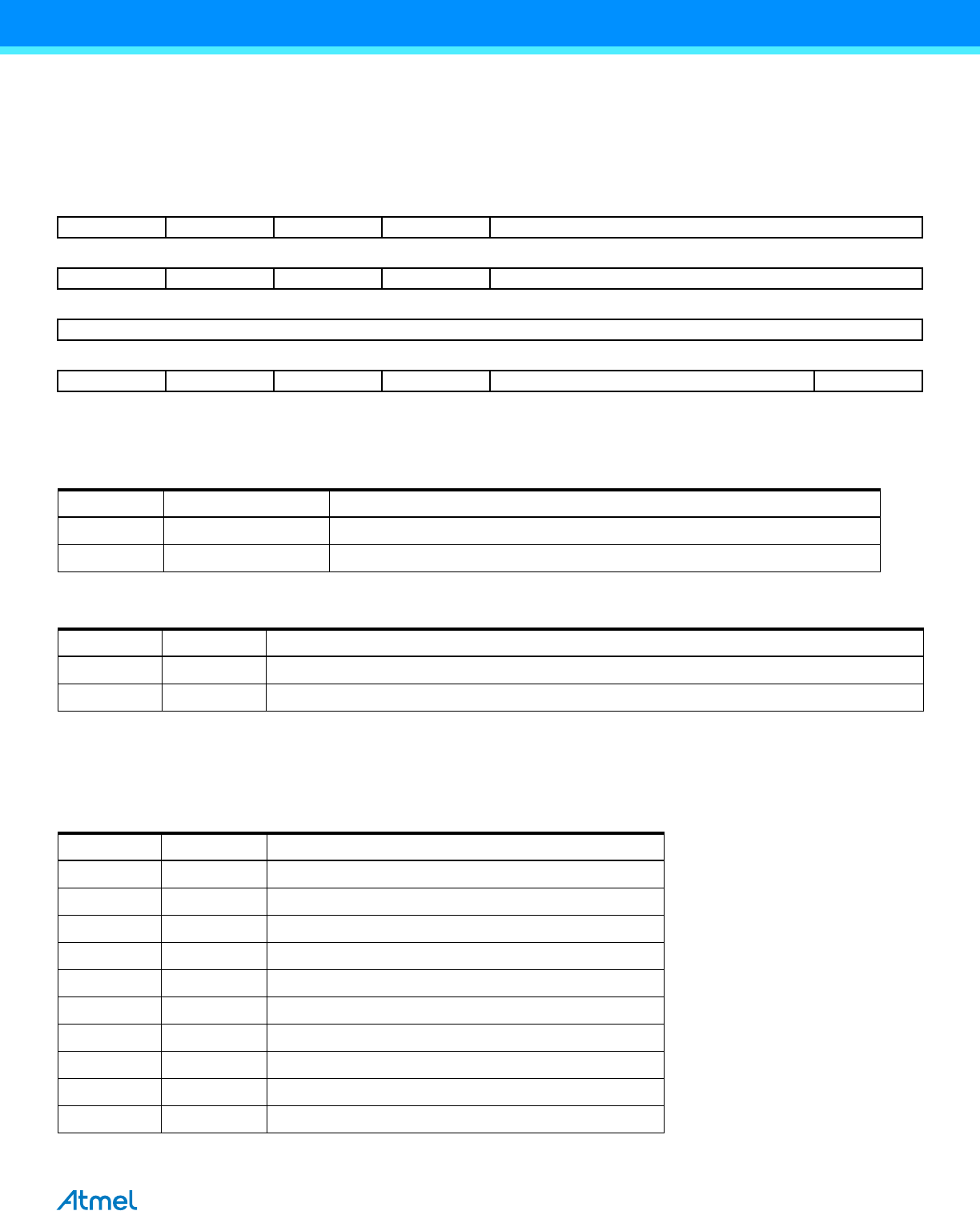
31 30 29 28 27 26 25 24
USEQ – – – TRACKTIM
23 22 21 20 19 18 17 16
–DIV1– – STARTUP
15 14 13 12 11 10 9 8
PRESCAL
76543210
–
– SLEEP LOWRES – –
Value Name Description
0 BITS_10 10-bit resolution.
1 BITS_8 8-bit resolution
Value Name Description
0 NORMAL Normal Mode: The ADC Core and reference voltage circuitry are kept ON between conversions
1 SLEEP Sleep Mode: The ADC Core and reference voltage circuitry are OFF between conversions
Value Name Description
0 SUT0 0 periods of ADCClock
1 SUT8 8 periods of ADCClock
2 SUT16 16 periods of ADCClock
3 SUT24 24 periods of ADCClock
4 SUT64 64 periods of ADCClock
5 SUT80 80 periods of ADCClock
6 SUT96 96 periods of ADCClock
7 SUT112 112 periods of ADCClock
8 SUT512 512 periods of ADCClock
9 SUT576 576 periods of ADCClock