
Datasheet


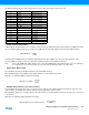


Table Of Contents
- Description
- 1. Features
- 2. Block Diagram
- 3. Signal Description
- 4. Package and Pinout
- 5. Power Considerations
- 6. Memories
- 7. System Controller
- 8. Peripherals
- 9. ARM926EJ-S Processor Overview
- 9.1 Description
- 9.2 Embedded Characteristics
- 9.3 Block Diagram
- 9.4 ARM9EJ-S Processor
- 9.5 CP15 Coprocessor
- 9.6 Memory Management Unit (MMU)
- 9.7 Caches and Write Buffer
- 9.8 Bus Interface Unit
- 10. Debug and Test
- 11. Advanced Interrupt Controller (AIC)
- 11.1 Description
- 11.2 Embedded Characteristics
- 11.3 Block Diagram
- 11.4 Application Block Diagram
- 11.5 AIC Detailed Block Diagram
- 11.6 I/O Line Description
- 11.7 Product Dependencies
- 11.8 Functional Description
- 11.9 Write Protection Registers
- 11.10 Advanced Interrupt Controller (AIC) User Interface
- 11.10.1 Base Address
- 11.10.2 AIC Source Mode Register
- 11.10.3 AIC Source Vector Register
- 11.10.4 AIC Interrupt Vector Register
- 11.10.5 AIC FIQ Vector Register
- 11.10.6 AIC Interrupt Status Register
- 11.10.7 AIC Interrupt Pending Register
- 11.10.8 AIC Interrupt Mask Register
- 11.10.9 AIC Core Interrupt Status Register
- 11.10.10 AIC Interrupt Enable Command Register
- 11.10.11 AIC Interrupt Disable Command Register
- 11.10.12 AIC Interrupt Clear Command Register
- 11.10.13 AIC Interrupt Set Command Register
- 11.10.14 AIC End of Interrupt Command Register
- 11.10.15 AIC Spurious Interrupt Vector Register
- 11.10.16 AIC Debug Control Register
- 11.10.17 AIC Fast Forcing Enable Register
- 11.10.18 AIC Fast Forcing Disable Register
- 11.10.19 AIC Fast Forcing Status Register
- 11.10.20 AIC Write Protect Mode Register
- 11.10.21 AIC Write Protect Status Register
- 12. Boot Strategies
- 13. Boot Sequence Controller (BSC)
- 14. Reset Controller (RSTC)
- 15. Real-time Clock (RTC)
- 15.1 Description
- 15.2 Embedded Characteristics
- 15.3 Block Diagram
- 15.4 Product Dependencies
- 15.5 Functional Description
- 15.6 Real-time Clock (RTC) User Interface
- 15.6.1 RTC Control Register
- 15.6.2 RTC Mode Register
- 15.6.3 RTC Time Register
- 15.6.4 RTC Calendar Register
- 15.6.5 RTC Time Alarm Register
- 15.6.6 RTC Calendar Alarm Register
- 15.6.7 RTC Status Register
- 15.6.8 RTC Status Clear Command Register
- 15.6.9 RTC Interrupt Enable Register
- 15.6.10 RTC Interrupt Disable Register
- 15.6.11 RTC Interrupt Mask Register
- 15.6.12 RTC Valid Entry Register
- 16. Periodic Interval Timer (PIT)
- 17. Watchdog Timer (WDT)
- 18. Shutdown Controller (SHDWC)
- 19. General-Purpose Backup Registers (GPBR)
- 20. Slow Clock Controller (SCKC)
- 21. Clock Generator
- 22. Power Management Controller (PMC)
- 22.1 Description
- 22.2 Embedded Characteristics
- 22.3 Block Diagram
- 22.4 Master Clock Controller
- 22.5 Processor Clock Controller
- 22.6 USB Device and Host Clocks
- 22.7 LP-DDR/DDR2 Clock
- 22.8 Peripheral Clock Controller
- 22.9 Programmable Clock Output Controller
- 22.10 Programming Sequence
- 22.11 Clock Switching Details
- 22.12 Power Management Controller (PMC) User Interface
- 22.12.1 PMC System Clock Enable Register
- 22.12.2 PMC System Clock Disable Register
- 22.12.3 PMC System Clock Status Register
- 22.12.4 PMC Peripheral Clock Enable Register
- 22.12.5 PMC Peripheral Clock Disable Register
- 22.12.6 PMC Peripheral Clock Status Register
- 22.12.7 PMC Clock Generator Main Oscillator Register
- 22.12.8 PMC Clock Generator Main Clock Frequency Register
- 22.12.9 PMC Clock Generator PLLA Register
- 22.12.10 PMC Clock Generator PLLB Register
- 22.12.11 PMC Master Clock Register
- 22.12.12 USB Clock Register
- 22.12.13 PMC Programmable Clock Register
- 22.12.14 PMC Interrupt Enable Register
- 22.12.15 PMC Interrupt Disable Register
- 22.12.16 PMC Status Register
- 22.12.17 PMC Interrupt Mask Register
- 22.12.18 PLL Charge Pump Current Register
- 22.12.19 PMC Write Protect Mode Register
- 22.12.20 PMC Write Protect Status Register
- 22.12.21 PMC Peripheral Control Register
- 23. Parallel Input/Output Controller (PIO)
- 23.1 Description
- 23.2 Embedded Characteristics
- 23.3 Block Diagram
- 23.4 Product Dependencies
- 23.5 Functional Description
- 23.5.1 Pull-up and Pull-down Resistor Control
- 23.5.2 I/O Line or Peripheral Function Selection
- 23.5.3 Peripheral A or B or C or D Selection
- 23.5.4 Output Control
- 23.5.5 Synchronous Data Output
- 23.5.6 Multi-Drive Control (Open Drain)
- 23.5.7 Output Line Timings
- 23.5.8 Inputs
- 23.5.9 Input Glitch and Debouncing Filters
- 23.5.10 Input Edge/Level Interrupt
- 23.5.11 Programmable I/O Delays
- 23.5.12 Programmable I/O Drive
- 23.5.13 Programmable Schmitt Trigger
- 23.5.14 Register Write Protection
- 23.6 I/O Lines Programming Example
- 23.7 Parallel Input/Output Controller (PIO) User Interface
- 23.7.1 PIO Enable Register
- 23.7.2 PIO Disable Register
- 23.7.3 PIO Status Register
- 23.7.4 PIO Output Enable Register
- 23.7.5 PIO Output Disable Register
- 23.7.6 PIO Output Status Register
- 23.7.7 PIO Input Filter Enable Register
- 23.7.8 PIO Input Filter Disable Register
- 23.7.9 PIO Input Filter Status Register
- 23.7.10 PIO Set Output Data Register
- 23.7.11 PIO Clear Output Data Register
- 23.7.12 PIO Output Data Status Register
- 23.7.13 PIO Pin Data Status Register
- 23.7.14 PIO Interrupt Enable Register
- 23.7.15 PIO Interrupt Disable Register
- 23.7.16 PIO Interrupt Mask Register
- 23.7.17 PIO Interrupt Status Register
- 23.7.18 PIO Multi-driver Enable Register
- 23.7.19 PIO Multi-driver Disable Register
- 23.7.20 PIO Multi-driver Status Register
- 23.7.21 PIO Pull-Up Disable Register
- 23.7.22 PIO Pull-Up Enable Register
- 23.7.23 PIO Pull-Up Status Register
- 23.7.24 PIO Peripheral ABCD Select Register 1
- 23.7.25 PIO Peripheral ABCD Select Register 2
- 23.7.26 PIO Input Filter Slow Clock Disable Register
- 23.7.27 PIO Input Filter Slow Clock Enable Register
- 23.7.28 PIO Input Filter Slow Clock Status Register
- 23.7.29 PIO Slow Clock Divider Debouncing Register
- 23.7.30 PIO Pad Pull-Down Disable Register
- 23.7.31 PIO Pad Pull-Down Enable Register
- 23.7.32 PIO Pad Pull-Down Status Register
- 23.7.33 PIO Output Write Enable Register
- 23.7.34 PIO Output Write Disable Register
- 23.7.35 PIO Output Write Status Register
- 23.7.36 PIO Additional Interrupt Modes Enable Register
- 23.7.37 PIO Additional Interrupt Modes Disable Register
- 23.7.38 PIO Additional Interrupt Modes Mask Register
- 23.7.39 PIO Edge Select Register
- 23.7.40 PIO Level Select Register
- 23.7.41 PIO Edge/Level Status Register
- 23.7.42 PIO Falling Edge/Low-Level Select Register
- 23.7.43 PIO Rising Edge/High-Level Select Register
- 23.7.44 PIO Fall/Rise - Low/High Status Register
- 23.7.45 PIO Write Protection Mode Register
- 23.7.46 PIO Write Protection Status Register
- 23.7.47 PIO Schmitt Trigger Register
- 23.7.48 PIO I/O Delay Register
- 23.7.49 PIO I/O Drive Register 1
- 23.7.50 PIO I/O Drive Register 2
- 24. Debug Unit (DBGU)
- 24.1 Description
- 24.2 Embedded Characteristics
- 24.3 Block Diagram
- 24.4 Product Dependencies
- 24.5 UART Operations
- 24.6 Debug Unit (DBGU) User Interface
- 24.6.1 Debug Unit Control Register
- 24.6.2 Debug Unit Mode Register
- 24.6.3 Debug Unit Interrupt Enable Register
- 24.6.4 Debug Unit Interrupt Disable Register
- 24.6.5 Debug Unit Interrupt Mask Register
- 24.6.6 Debug Unit Status Register
- 24.6.7 Debug Unit Receiver Holding Register
- 24.6.8 Debug Unit Transmit Holding Register
- 24.6.9 Debug Unit Baud Rate Generator Register
- 24.6.10 Debug Unit Chip ID Register
- 24.6.11 Debug Unit Chip ID Extension Register
- 24.6.12 Debug Unit Force NTRST Register
- 25. Fuse Controller (FUSE)
- 26. Bus Matrix (MATRIX)
- 26.1 Description
- 26.2 Embedded Characteristics
- 26.3 Matrix Masters
- 26.4 Matrix Slaves
- 26.5 Master to Slave Access
- 26.6 Memory Mapping
- 26.7 Special Bus Granting Mechanism
- 26.8 Arbitration
- 26.9 Write Protect Registers
- 26.10 Bus Matrix (MATRIX) User Interface
- 26.10.1 Bus Matrix Master Configuration Registers
- 26.10.2 Bus Matrix Slave Configuration Registers
- 26.10.3 Bus Matrix Priority Registers A For Slaves
- 26.10.4 Bus Matrix Master Remap Control Register
- 26.10.5 Chip Configuration User Interface
- 26.10.6 Write Protect Mode Register
- 26.10.7 Write Protect Status Register
- 27. External Bus Interface (EBI)
- 27.1 Description
- 27.2 Embedded Characteristics
- 27.3 EBI Block Diagram
- 27.4 I/O Lines Description
- 27.5 Application Example
- 27.6 Product Dependencies
- 27.7 Functional Description
- 27.8 Implementation Examples
- 28. Programmable Multibit ECC Controller (PMECC)
- 28.1 Description
- 28.2 Embedded Characteristics
- 28.3 Block Diagram
- 28.4 Functional Description
- 28.5 Software Implementation
- 28.6 Programmable Multibit ECC Controller (PMECC) User Interface
- 28.6.1 PMECC Configuration Register
- 28.6.2 PMECC Spare Area Size Register
- 28.6.3 PMECC Start Address Register
- 28.6.4 PMECC End Address Register
- 28.6.5 PMECC Clock Control Register
- 28.6.6 PMECC Control Register
- 28.6.7 PMECC Status Register
- 28.6.8 PMECC Interrupt Enable Register
- 28.6.9 PMECC Interrupt Disable Register
- 28.6.10 PMECC Interrupt Mask Register
- 28.6.11 PMECC Interrupt Status Register
- 28.6.12 PMECC ECC x Register
- 28.6.13 PMECC Remainder x Register
- 29. Programmable Multibit ECC Error Location Controller (PMERRLOC)
- 29.1 Description
- 29.2 Embedded Characteristics
- 29.3 Block Diagram
- 29.4 Functional Description
- 29.5 Programmable Multibit ECC Error Location (PMERRLOC) User Interface
- 29.5.1 Error Location Configuration Register
- 29.5.2 Error Location Primitive Register
- 29.5.3 Error Location Enable Register
- 29.5.4 Error Location Disable Register
- 29.5.5 Error Location Status Register
- 29.5.6 Error Location Interrupt Enable Register
- 29.5.7 Error Location Interrupt Disable Register
- 29.5.8 Error Location Interrupt Mask Register
- 29.5.9 Error Location Interrupt Status Register
- 29.5.10 Error Location SIGMAx Register
- 29.5.11 PMECC Error Locationx Register
- 30. Static Memory Controller (SMC)
- 30.1 Description
- 30.2 Embedded Characteristics
- 30.3 I/O Lines Description
- 30.4 Multiplexed Signals
- 30.5 Application Example
- 30.6 Product Dependencies
- 30.7 External Memory Mapping
- 30.8 Connection to External Devices
- 30.9 Standard Read and Write Protocols
- 30.10 Automatic Wait States
- 30.11 Data Float Wait States
- 30.12 External Wait
- 30.13 Slow Clock Mode
- 30.14 Asynchronous Page Mode
- 30.15 Programmable IO Delays
- 30.16 Static Memory Controller (SMC) User Interface
- 31. DDR SDR SDRAM Controller (DDRSDRC)
- 31.1 Description
- 31.2 Embedded Characteristics
- 31.3 DDRSDRC Module Diagram
- 31.4 Initialization Sequence
- 31.5 Functional Description
- 31.6 Software Interface/SDRAM Organization, Address Mapping
- 31.7 DDR SDR SDRAM Controller (DDRSDRC) User Interface
- 31.7.1 DDRSDRC Mode Register
- 31.7.2 DDRSDRC Refresh Timer Register
- 31.7.3 DDRSDRC Configuration Register
- 31.7.4 DDRSDRC Timing Parameter 0 Register
- 31.7.5 DDRSDRC Timing Parameter 1 Register
- 31.7.6 DDRSDRC Timing Parameter 2 Register
- 31.7.7 DDRSDRC Low-power Register
- 31.7.8 DDRSDRC Memory Device Register
- 31.7.9 DDRSDRC DLL Register
- 31.7.10 DDRSDRC High Speed Register
- 31.7.11 DDRSDRC Write Protect Mode Register
- 31.7.12 DDRSDRC Write Protect Status Register
- 32. DMA Controller (DMAC)
- 32.1 Description
- 32.2 Embedded Characteristics
- 32.3 DMA Controller Peripheral Connections
- 32.4 Block Diagram
- 32.5 Functional Description
- 32.6 DMAC Software Requirements
- 32.7 Write Protection Registers
- 32.8 DMA Controller (DMAC) User Interface
- 32.8.1 DMAC Global Configuration Register
- 32.8.2 DMAC Enable Register
- 32.8.3 DMAC Software Single Request Register
- 32.8.4 DMAC Software Chunk Transfer Request Register
- 32.8.5 DMAC Software Last Transfer Flag Register
- 32.8.6 DMAC Error, Buffer Transfer and Chained Buffer Transfer Interrupt Enable Register
- 32.8.7 DMAC Error, Buffer Transfer and Chained Buffer Transfer Interrupt Disable Register
- 32.8.8 DMAC Error, Buffer Transfer and Chained Buffer Transfer Interrupt Mask Register
- 32.8.9 DMAC Error, Buffer Transfer and Chained Buffer Transfer Status Register
- 32.8.10 DMAC Channel Handler Enable Register
- 32.8.11 DMAC Channel Handler Disable Register
- 32.8.12 DMAC Channel Handler Status Register
- 32.8.13 DMAC Channel x [x = 0..7] Source Address Register
- 32.8.14 DMAC Channel x [x = 0..7] Destination Address Register
- 32.8.15 DMAC Channel x [x = 0..7] Descriptor Address Register
- 32.8.16 DMAC Channel x [x = 0..7] Control A Register
- 32.8.17 DMAC Channel x [x = 0..7] Control B Register
- 32.8.18 DMAC Channel x [x = 0..7] Configuration Register
- 32.8.19 DMAC Channel x [x = 0..7] Source Picture-in-Picture Configuration Register
- 32.8.20 DMAC Channel x [x = 0..7] Destination Picture-in-Picture Configuration Register
- 32.8.21 DMAC Write Protect Mode Register
- 32.8.22 DMAC Write Protect Status Register
- 33. USB Device Port (UDP)
- 33.1 Description
- 33.2 Embedded Characteristics
- 33.3 Block Diagram
- 33.4 Product Dependencies
- 33.5 Typical Connection
- 33.6 Functional Description
- 33.7 USB Device Port (UDP) User Interface
- 33.7.1 UDP Frame Number Register
- 33.7.2 UDP Global State Register
- 33.7.3 UDP Function Address Register
- 33.7.4 UDP Interrupt Enable Register
- 33.7.5 UDP Interrupt Disable Register
- 33.7.6 UDP Interrupt Mask Register
- 33.7.7 UDP Interrupt Status Register
- 33.7.8 UDP Interrupt Clear Register
- 33.7.9 UDP Reset Endpoint Register
- 33.7.10 UDP Endpoint Control and Status Register (Control, Bulk Interrupt Endpoints)
- 33.7.11 UDP Endpoint Control and Status Register (Isochronous Endpoints)
- 33.7.12 UDP FIFO Data Register
- 33.7.13 UDP Transceiver Control Register
- 34. USB Host Port (UHP)
- 35. High Speed MultiMedia Card Interface (HSMCI)
- 35.1 Description
- 35.2 Embedded Characteristics
- 35.3 Block Diagram
- 35.4 Application Block Diagram
- 35.5 Pin Name List
- 35.6 Product Dependencies
- 35.7 Bus Topology
- 35.8 High Speed MultiMedia Card Operations
- 35.9 SD/SDIO Card Operation
- 35.10 CE-ATA Operation
- 35.11 HSMCI Boot Operation Mode
- 35.12 HSMCI Transfer Done Timings
- 35.13 Register Write Protection
- 35.14 High Speed MultiMedia Card Interface (HSMCI) User Interface
- 35.14.1 HSMCI Control Register
- 35.14.2 HSMCI Mode Register
- 35.14.3 HSMCI Data Timeout Register
- 35.14.4 HSMCI SDCard/SDIO Register
- 35.14.5 HSMCI Argument Register
- 35.14.6 HSMCI Command Register
- 35.14.7 HSMCI Block Register
- 35.14.8 HSMCI Completion Signal Timeout Register
- 35.14.9 HSMCI Response Register
- 35.14.10 HSMCI Receive Data Register
- 35.14.11 HSMCI Transmit Data Register
- 35.14.12 HSMCI Status Register
- 35.14.13 HSMCI Interrupt Enable Register
- 35.14.14 HSMCI Interrupt Disable Register
- 35.14.15 HSMCI Interrupt Mask Register
- 35.14.16 HSMCI DMA Configuration Register
- 35.14.17 HSMCI Configuration Register
- 35.14.18 HSMCI Write Protection Mode Register
- 35.14.19 HSMCI Write Protection Status Register
- 35.14.20 HSMCI FIFOx Memory Aperture
- 36. Serial Peripheral Interface (SPI)
- 36.1 Description
- 36.2 Embedded Characteristics
- 36.3 Block Diagram
- 36.4 Application Block Diagram
- 36.5 Signal Description
- 36.6 Product Dependencies
- 36.7 Functional Description
- 36.7.1 Modes of Operation
- 36.7.2 Data Transfer
- 36.7.3 Master Mode Operations
- 36.7.3.1 Master Mode Block Diagram
- 36.7.3.2 Master Mode Flow Diagram
- 36.7.3.3 Clock Generation
- 36.7.3.4 Transfer Delays
- 36.7.3.5 Peripheral Selection
- 36.7.3.6 SPI Direct Access Memory Controller (DMAC)
- 36.7.3.7 Peripheral Chip Select Decoding
- 36.7.3.8 Peripheral Deselection without DMA
- 36.7.3.9 Peripheral Deselection with DMAC
- 36.7.3.10 Mode Fault Detection
- 36.7.4 SPI Slave Mode
- 36.7.5 Write Protected Registers
- 36.8 Serial Peripheral Interface (SPI) User Interface
- 36.8.1 SPI Control Register
- 36.8.2 SPI Mode Register
- 36.8.3 SPI Receive Data Register
- 36.8.4 SPI Transmit Data Register
- 36.8.5 SPI Status Register
- 36.8.6 SPI Interrupt Enable Register
- 36.8.7 SPI Interrupt Disable Register
- 36.8.8 SPI Interrupt Mask Register
- 36.8.9 SPI Chip Select Register
- 36.8.10 SPI Write Protection Mode Register
- 36.8.11 SPI Write Protection Status Register
- 37. Timer Counter (TC)
- 37.1 Description
- 37.2 Embedded Characteristics
- 37.3 Block Diagram
- 37.4 Pin Name List
- 37.5 Product Dependencies
- 37.6 Functional Description
- 37.6.1 TC Description
- 37.6.2 32-bit Counter
- 37.6.3 Clock Selection
- 37.6.4 Clock Control
- 37.6.5 TC Operating Modes
- 37.6.6 Trigger
- 37.6.7 Capture Operating Mode
- 37.6.8 Capture Registers A and B
- 37.6.9 Transfer with DMAC
- 37.6.10 Trigger Conditions
- 37.6.11 Waveform Operating Mode
- 37.6.12 Waveform Selection
- 37.6.13 External Event/Trigger Conditions
- 37.6.14 Output Controller
- 37.7 Timer Counter (TC) User Interface
- 37.7.1 TC Channel Control Register
- 37.7.2 TC Channel Mode Register: Capture Mode
- 37.7.3 TC Channel Mode Register: Waveform Mode
- 37.7.4 TC Register AB
- 37.7.5 TC Counter Value Register
- 37.7.6 TC Register A
- 37.7.7 TC Register B
- 37.7.8 TC Register C
- 37.7.9 TC Status Register
- 37.7.10 TC Interrupt Enable Register
- 37.7.11 TC Interrupt Disable Register
- 37.7.12 TC Interrupt Mask Register
- 37.7.13 TC Block Control Register
- 37.7.14 TC Block Mode Register
- 38. Pulse Width Modulation Controller (PWM)
- 38.1 Description
- 38.2 Embedded characteristics
- 38.3 Block Diagram
- 38.4 I/O Lines Description
- 38.5 Product Dependencies
- 38.6 Functional Description
- 38.7 Pulse Width Modulation Controller (PWM) User Interface
- 38.7.1 PWM Mode Register
- 38.7.2 PWM Enable Register
- 38.7.3 PWM Disable Register
- 38.7.4 PWM Status Register
- 38.7.5 PWM Interrupt Enable Register
- 38.7.6 PWM Interrupt Disable Register
- 38.7.7 PWM Interrupt Mask Register
- 38.7.8 PWM Interrupt Status Register
- 38.7.9 PWM Channel Mode Register
- 38.7.10 PWM Channel Duty Cycle Register
- 38.7.11 PWM Channel Period Register
- 38.7.12 PWM Channel Counter Register
- 38.7.13 PWM Channel Update Register
- 39. Two-wire Interface (TWI)
- 39.1 Description
- 39.2 Embedded Characteristics
- 39.3 List of Abbreviations
- 39.4 Block Diagram
- 39.5 Application Block Diagram
- 39.6 Product Dependencies
- 39.7 Functional Description
- 39.8 Master Mode
- 39.9 Multi-master Mode
- 39.10 Slave Mode
- 39.11 Write Protection System
- 39.12 Two-wire Interface (TWI) User Interface
- 39.12.1 TWI Control Register
- 39.12.2 TWI Master Mode Register
- 39.12.3 TWI Slave Mode Register
- 39.12.4 TWI Internal Address Register
- 39.12.5 TWI Clock Waveform Generator Register
- 39.12.6 TWI Status Register
- 39.12.7 TWI Interrupt Enable Register
- 39.12.8 TWI Interrupt Disable Register
- 39.12.9 TWI Interrupt Mask Register
- 39.12.10 TWI Receive Holding Register
- 39.12.11 TWI Transmit Holding Register
- 39.12.12 TWI Write Protection Mode Register
- 39.12.13 TWI Write Protection Status Register
- 40. Universal Synchronous Asynchronous Receiver Transceiver (USART)
- 40.1 Description
- 40.2 Embedded Characteristics
- 40.3 Block Diagram
- 40.4 Application Block Diagram
- 40.5 I/O Lines Description
- 40.6 Product Dependencies
- 40.7 Functional Description
- 40.7.1 Baud Rate Generator
- 40.7.2 Receiver and Transmitter Control
- 40.7.3 Synchronous and Asynchronous Modes
- 40.7.3.1 Transmitter Operations
- 40.7.3.2 Manchester Encoder
- 40.7.3.3 Asynchronous Receiver
- 40.7.3.4 Manchester Decoder
- 40.7.3.5 Radio Interface: Manchester Encoded USART Application
- 40.7.3.6 Synchronous Receiver
- 40.7.3.7 Receiver Operations
- 40.7.3.8 Parity
- 40.7.3.9 Multidrop Mode
- 40.7.3.10 Transmitter Timeguard
- 40.7.3.11 Receiver Time-out
- 40.7.3.12 Framing Error
- 40.7.3.13 Transmit Break
- 40.7.3.14 Receive Break
- 40.7.3.15 Hardware Handshaking
- 40.7.4 ISO7816 Mode
- 40.7.5 IrDA Mode
- 40.7.6 RS485 Mode
- 40.7.7 SPI Mode
- 40.7.8 LIN Mode
- 40.7.8.1 Modes of Operation
- 40.7.8.2 Baud Rate Configuration
- 40.7.8.3 Receiver and Transmitter Control
- 40.7.8.4 Character Transmission
- 40.7.8.5 Character Reception
- 40.7.8.6 Header Transmission (Master Node Configuration)
- 40.7.8.7 Header Reception (Slave Node Configuration)
- 40.7.8.8 Slave Node Synchronization
- 40.7.8.9 Identifier Parity
- 40.7.8.10 Node Action
- 40.7.8.11 Response Data Length
- 40.7.8.12 Checksum
- 40.7.8.13 Frame Slot Mode
- 40.7.8.14 LIN Errors
- 40.7.8.15 LIN Frame Handling
- 40.7.8.16 LIN Frame Handling With the DMAC
- 40.7.8.17 Wake-up Request
- 40.7.8.18 Bus Idle Time-out
- 40.7.9 Test Modes
- 40.7.10 Write Protection Registers
- 40.8 Universal Synchronous Asynchronous Receiver Transmitter (USART) User Interface
- 40.8.1 USART Control Register
- 40.8.2 USART Control Register (SPI_MODE)
- 40.8.3 USART Mode Register
- 40.8.4 USART Mode Register (SPI_MODE)
- 40.8.5 USART Interrupt Enable Register
- 40.8.6 USART Interrupt Enable Register (SPI_MODE)
- 40.8.7 USART Interrupt Enable Register (LIN_MODE)
- 40.8.8 USART Interrupt Disable Register
- 40.8.9 USART Interrupt Disable Register (SPI_MODE)
- 40.8.10 USART Interrupt Disable Register (LIN_MODE)
- 40.8.11 USART Interrupt Mask Register
- 40.8.12 USART Interrupt Mask Register (SPI_MODE)
- 40.8.13 USART Interrupt Mask Register (LIN_MODE)
- 40.8.14 USART Channel Status Register
- 40.8.15 USART Channel Status Register (SPI_MODE)
- 40.8.16 USART Channel Status Register (LIN_MODE)
- 40.8.17 USART Receive Holding Register
- 40.8.18 USART Transmit Holding Register
- 40.8.19 USART Baud Rate Generator Register
- 40.8.20 USART Receiver Time-out Register
- 40.8.21 USART Transmitter Timeguard Register
- 40.8.22 USART FI DI RATIO Register
- 40.8.23 USART Number of Errors Register
- 40.8.24 USART IrDA FILTER Register
- 40.8.25 USART Manchester Configuration Register
- 40.8.26 USART LIN Mode Register
- 40.8.27 USART LIN Identifier Register
- 40.8.28 USART LIN Baud Rate Register
- 40.8.29 USART Write Protect Mode Register
- 40.8.30 USART Write Protect Status Register
- 41. Universal Asynchronous Receiver Transmitter (UART)
- 41.1 Description
- 41.2 Embedded Characteristics
- 41.3 Block Diagram
- 41.4 Product Dependencies
- 41.5 UART Operations
- 41.6 Universal Asynchronous Receiver Transmitter (UART) User Interface
- 41.6.1 UART Control Register
- 41.6.2 UART Mode Register
- 41.6.3 UART Interrupt Enable Register
- 41.6.4 UART Interrupt Disable Register
- 41.6.5 UART Interrupt Mask Register
- 41.6.6 UART Status Register
- 41.6.7 UART Receiver Holding Register
- 41.6.8 UART Transmit Holding Register
- 41.6.9 UART Baud Rate Generator Register
- 42. Analog-to-Digital Converter (ADC)
- 42.1 Description
- 42.2 Embedded Characteristics
- 42.3 Block Diagram
- 42.4 Signal Description
- 42.5 Product Dependencies
- 42.6 Functional Description
- 42.7 Touchscreen
- 42.7.1 Touchscreen Mode
- 42.7.2 4-wire Resistive Touchscreen Principles
- 42.7.3 4-wire Position Measurement Method
- 42.7.4 4-wire Pressure Measurement Method
- 42.7.5 5-wire Resistive Touchscreen Principles
- 42.7.6 5-wire Position Measurement Method
- 42.7.7 Sequence and Noise Filtering
- 42.7.8 Measured Values, Registers and Flags
- 42.7.9 Pen Detect Method
- 42.7.10 Buffer Structure
- 42.7.11 Write Protected Registers
- 42.8 Analog-to-Digital Converter (ADC) User Interface
- 42.8.1 ADC Control Register
- 42.8.2 ADC Mode Register
- 42.8.3 ADC Channel Sequence 1 Register
- 42.8.4 ADC Channel Sequence 2 Register
- 42.8.5 ADC Channel Enable Register
- 42.8.6 ADC Channel Disable Register
- 42.8.7 ADC Channel Status Register
- 42.8.8 ADC Last Converted Data Register
- 42.8.9 ADC Interrupt Enable Register
- 42.8.10 ADC Interrupt Disable Register
- 42.8.11 ADC Interrupt Mask Register
- 42.8.12 ADC Interrupt Status Register
- 42.8.13 ADC Overrun Status Register
- 42.8.14 ADC Extended Mode Register
- 42.8.15 ADC Compare Window Register
- 42.8.16 ADC Channel Data Register
- 42.8.17 ADC Analog Control Register
- 42.8.18 ADC Touchscreen Mode Register
- 42.8.19 ADC Touchscreen X Position Register
- 42.8.20 ADC Touchscreen Y Position Register
- 42.8.21 ADC Touchscreen Pressure Register
- 42.8.22 ADC Trigger Register
- 42.8.23 ADC Write Protect Mode Register
- 42.8.24 ADC Write Protect Status Register
- 43. Synchronous Serial Controller (SSC)
- 43.1 Description
- 43.2 Embedded Characteristics
- 43.3 Block Diagram
- 43.4 Application Block Diagram
- 43.5 Pin Name List
- 43.6 Product Dependencies
- 43.7 Functional Description
- 43.8 SSC Application Examples
- 43.9 Synchronous Serial Controller (SSC) User Interface
- 43.9.1 SSC Control Register
- 43.9.2 SSC Clock Mode Register
- 43.9.3 SSC Receive Clock Mode Register
- 43.9.4 SSC Receive Frame Mode Register
- 43.9.5 SSC Transmit Clock Mode Register
- 43.9.6 SSC Transmit Frame Mode Register
- 43.9.7 SSC Receive Holding Register
- 43.9.8 SSC Transmit Holding Register
- 43.9.9 SSC Receive Synchronization Holding Register
- 43.9.10 SSC Transmit Synchronization Holding Register
- 43.9.11 SSC Receive Compare 0 Register
- 43.9.12 SSC Receive Compare 1 Register
- 43.9.13 SSC Status Register
- 43.9.14 SSC Interrupt Enable Register
- 43.9.15 SSC Interrupt Disable Register
- 43.9.16 SSC Interrupt Mask Register
- 43.9.17 SSC Write Protect Mode Register
- 43.9.18 SSC Write Protect Status Register
- 44. LCD Controller (LCDC)
- 44.1 Description
- 44.2 Embedded Characteristics
- 44.3 Block Diagram
- 44.4 I/O Lines Description
- 44.5 Product Dependencies
- 44.6 Functional Description
- 44.6.1 Timing Engine Configuration
- 44.6.2 DMA Software Operations
- 44.6.3 Display Software Configuration
- 44.6.4 RGB Frame Buffer Memory Bitmap
- 44.6.4.1 1 bpp Through Color Lookup Table
- 44.6.4.2 2 bpp Through Color Lookup Table
- 44.6.4.3 4 bpp Through Color Lookup Table
- 44.6.4.4 8 bpp Through Color Lookup Table
- 44.6.4.5 12 bpp Memory Mapping, RGB 4:4:4
- 44.6.4.6 16 bpp Memory Mapping with Alpha Channel, ARGB 4:4:4:4
- 44.6.4.7 16 bpp Memory Mapping with Alpha Channel, RGBA 4:4:4:4
- 44.6.4.8 16 bpp Memory Mapping with Alpha Channel, RGB 5:6:5
- 44.6.4.9 16 bpp Memory Mapping with Transparency Bit, ARGB 1:5:5:5
- 44.6.4.10 18 bpp Unpacked Memory Mapping with Transparency Bit, RGB 6:6:6
- 44.6.4.11 18 bpp Packed Memory Mapping with Transparency Bit, RGB 6:6:6
- 44.6.4.12 19 bpp Unpacked Memory Mapping with Transparency Bit, RGB 1:6:6:6
- 44.6.4.13 19 bpp Packed Memory Mapping with Transparency Bit, ARGB 1:6:6:6
- 44.6.4.14 24 bpp Unpacked Memory Mapping, RGB 8:8:8
- 44.6.4.15 24 bpp Packed Memory Mapping, RGB 8:8:8
- 44.6.4.16 25 bpp Memory Mapping, ARGB 1:8:8:8
- 44.6.4.17 32 bpp Memory Mapping, ARGB 8:8:8:8
- 44.6.4.18 32 bpp Memory Mapping, RGBA 8:8:8:8
- 44.6.5 Output Timing Generation
- 44.6.6 Output Format
- 44.7 LCD Controller (LCDC) User Interface
- 44.7.1 LCD Controller Configuration Register 0
- 44.7.2 LCD Controller Configuration Register 1
- 44.7.3 LCD Controller Configuration Register 2
- 44.7.4 LCD Controller Configuration Register 3
- 44.7.5 LCD Controller Configuration Register 4
- 44.7.6 LCD Controller Configuration Register 5
- 44.7.7 LCD Controller Configuration Register 6
- 44.7.8 LCD Controller Enable Register
- 44.7.9 LCD Controller Disable Register
- 44.7.10 LCD Controller Status Register
- 44.7.11 LCD Controller Interrupt Enable Register
- 44.7.12 LCD Controller Interrupt Disable Register
- 44.7.13 LCD Controller Interrupt Mask Register
- 44.7.14 LCD Controller Interrupt Status Register
- 44.7.15 Base Layer Channel Enable Register
- 44.7.16 Base Layer Channel Disable Register
- 44.7.17 Base Layer Channel Status Register
- 44.7.18 Base Layer Interrupt Enable Register
- 44.7.19 Base Layer Interrupt Disable Register
- 44.7.20 Base Layer Interrupt Mask Register
- 44.7.21 Base Layer Interrupt Status Register
- 44.7.22 Base Layer Head Register
- 44.7.23 Base Layer Address Register
- 44.7.24 Base Layer Control Register
- 44.7.25 Base Layer Next Register
- 44.7.26 Base Layer Configuration 0 Register
- 44.7.27 Base Layer Configuration 1 Register
- 44.7.28 Base Layer Configuration 2 Register
- 44.7.29 Base Layer Configuration 3 Register
- 44.7.30 Base Layer Configuration 4 Register
- 44.7.31 Base CLUT Register x Register
- 45. Advanced Encryption Standard (AES)
- 45.1 Description
- 45.2 Embedded Characteristics
- 45.3 Product Dependencies
- 45.4 Functional Description
- 45.5 Security Features
- 45.6 Advanced Encryption Standard (AES) User Interface
- 45.6.1 AES Control Register
- 45.6.2 AES Mode Register
- 45.6.3 AES Interrupt Enable Register
- 45.6.4 AES Interrupt Disable Register
- 45.6.5 AES Interrupt Mask Register
- 45.6.6 AES Interrupt Status Register
- 45.6.7 AES Key Word Register x
- 45.6.8 AES Input Data Register x
- 45.6.9 AES Output Data Register x
- 45.6.10 AES Initialization Vector Register x
- 46. Secure Hash Algorithm (SHA)
- 47. True Random Number Generator (TRNG)
- 48. Electrical Characteristics
- 48.1 Absolute Maximum Ratings
- 48.2 DC Characteristics
- 48.3 Power Consumption
- 48.4 Clock Characteristics
- 48.5 12 MHz RC Oscillator Characteristics
- 48.6 32 kHz Oscillator Characteristics
- 48.7 32 kHz RC Oscillator Characteristics
- 48.8 PLL Characteristics
- 48.9 I/Os
- 48.10 Analog-to-Digital Converter (ADC)
- 48.11 USB Transceiver Characteristics
- 48.12 Core Power Supply POR Characteristics
- 48.13 SMC Timings
- 48.14 DDRSDRC Timings
- 48.15 Peripheral Timings
- 49. Mechanical Overview of the 217-ball and 247-ball BGA Packages
- 50. SAM9N12/SAM9CN11/SAM9CN12 Ordering Information
- 51. SAM9N/CN Series Errata
- Revision History
- Table of Contents
642
SAM9N12/SAM9CN11/SAM9CN12 [DATASHEET]
11063K–ATARM–05-Nov-13
36.8.9 SPI Chip Select Register
Name: SPI_CSRx[x=0..3]
Addresses: 0xF0000030 (0), 0xF0004030 (1)
Access: Read/Write
This register can only be written if the WPEN bit is cleared in ”SPI Write Protection Mode Register”.
Note: SPI_CSRx registers must be written even if the user wants to use the defaults. The BITS field will not be updated with
the translated value unless the register is written.
• CPOL: Clock Polarity
0 = The inactive state value of SPCK is logic level zero.
1 = The inactive state value of SPCK is logic level one.
CPOL is used to determine the inactive state value of the serial clock (SPCK). It is used with NCPHA to produce the required
clock/data relationship between master and slave devices.
• NCPHA: Clock Phase
0 = Data is changed on the leading edge of SPCK and captured on the following edge of SPCK.
1 = Data is captured on the leading edge of SPCK and changed on the following edge of SPCK.
NCPHA determines which edge of SPCK causes data to change and which edge causes data to be captured. NCPHA is used
with CPOL to produce the required clock/data relationship between master and slave devices.
• CSNAAT: Chip Select Not Active After Transfer (Ignored if CSAAT = 1)
0 = The Peripheral Chip Select does not rise between two transfers if the SPI_TDR is reloaded before the end of the first transfer
and if the two transfers occur on the same Chip Select.
1 = The Peripheral Chip Select rises systematically after each transfer performed on the same slave. It remains active after the
end of transfer for a minimal duration of:
– (if DLYBCT field is different from 0)
– (if DLYBCT field equals 0)
• CSAAT: Chip Select Active After Transfer
0 = The Peripheral Chip Select Line rises as soon as the last transfer is achieved.
1 = The Peripheral Chip Select does not rise after the last transfer is achieved. It remains active until a new transfer is requested
on a different chip select.
• BITS: Bits Per Transfer
(See the
(Note:)
below the register table; Section 36.8.9 “SPI Chip Select Register” on page 642.)
31 30 29 28 27 26 25 24
DLYBCT
23 22 21 20 19 18 17 16
DLYBS
15 14 13 12 11 10 9 8
SCBR
76543210
BITS CSAAT CSNAAT NCPHA CPOL
DLYBCT
MCK
-----------------------
DLYBCT 1+
MCK
---------------------------------