
Datasheet


4
SAM9M10 [SUMMARY]
6355ES–ATARM–12-Mar-13
3. Signal Description
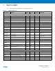
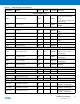
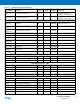
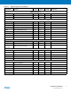
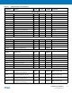
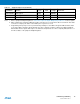
Table 3-1 gives details on the signal names classified by peripheral.
Table 3-1. Signal Description List
Signal Name Function Type
Active
Level
Reference
Voltage Comments
Power Supplies
VDDIOM0 DDR2 I/O Lines Power Supply Power 1.65V to 1.95V
VDDIOM1 EBI I/O Lines Power Supply Power 1.65V to 1.95V or 3.0V to3.6V
VDDIOP0 Peripherals I/O Lines Power Supply Power 1.65V to 3.6V
VDDIOP1 Peripherals I/O Lines Power Supply Power 1.65V to 3.6V
VDDIOP2 ISI I/O Lines Power Supply Power 1.65V to 3.6V
VDDBU Backup I/O Lines Power Supply Power 1.8V to 3.6V
VDDANA Analog Power Supply Power 3.0V to 3.6V
VDDPLLA PLLA Power Supply Power 0.9V to 1.1V
VDDPLLUTMI PLLUTMI Power Supply Power 0.9V to 1.1V
VDDOSC Oscillator Power Supply Power 1.65V to 3.6V
VDDCORE Core Chip Power Supply Power 0.9V to 1.1V
VDDUTMIC
UDPHS and UHPHS UTMI+ Core
Power Supply
Power 0.9V to 1.1V
VDDUTMII
UDPHS and UHPHS UTMI+ interface
Power Supply
Power 3.0V to 3.6V
GNDIOM DDR2 and EBI I/O Lines Ground Ground
GNDIOP Peripherals and ISI I/O lines Ground Ground
GNDCORE Core Chip Ground Ground
GNDOSC
PLLA, PLLUTMI and Oscillator
Ground
Ground
GNDBU Backup Ground Ground
GNDUTMI
UDPHS and UHPHS UTMI+ Core and
interface Ground
Ground
GNDANA Analog Ground Ground
Clocks, Oscillators and PLLs
XIN Main Oscillator Input Input
XOUT Main Oscillator Output Output
XIN32 Slow Clock Oscillator Input Input
XOUT32 Slow Clock Oscillator Output Output
VBG Bias Voltage Reference for USB Analog
PCK0 - PCK1 Programmable Clock Output Output
(1)