ARM-based Embedded MPU SAM9M10 SUMMARY Description The SAM9M10 is a multimedia enabled mid-range ARM926-based embedded MPU running at 400MHz, combining user interfaces, video playback and connectivity. It includes hardware video decoder, LCD Controller, resistive touchscreen, camera interface, audio, Ethernet 10/100 and high speed USB and SDIO. The hardware video decoder supports H.264, MPEG-4, MPEG-2, VC-1, H.263.
1.
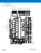
MCI0/MCI1 SD/SDI C ATA FIF T I0 T I1 PI PI B PI C PI D RSTC RTC RTT 4 GPBR PIT PI A P R P R SHDC SC 32K RC DT SC12M PLLUTMI PMC PLLA PDC DBGU AIC System Controller K TD I TD TM TCS K RT C T RS NT PDC USART0 USART1 USART2 USART3 R M 64KB SRAM 64KB 4-CH P M I TC0 TC1 TC2 D DCache ICache MMU 32Kbytes 32K bytes ITCM DTCM Bus Interface ARM926EJ-S In-Circuit mulator L TAG S TAG / Boundary Scan S PB TC3 TC4 TC5 DMA DMA HS USB HS Transceiver DMA LCD PI SPI0 SPI1 PDC
3. Signal Description Table 3-1 gives details on the signal names classified by peripheral. Table 3-1. Signal Description List Signal Name Function Type Active Level Reference Voltage Comments Power Supplies VDDIOM0 DDR2 I/O Lines Power Supply Power 1.65V to 1.95V VDDIOM1 EBI I/O Lines Power Supply Power 1.65V to 1.95V or 3.0V to3.6V VDDIOP0 Peripherals I/O Lines Power Supply Power 1.65V to 3.6V VDDIOP1 Peripherals I/O Lines Power Supply Power 1.65V to 3.
Table 3-1. Signal Description List (Continued) Signal Name Function Type Active Level Reference Voltage Comments VDDBU Driven at 0V only. 0: The device is in backup mode Shutdown, Wakeup Logic SHDN Shut-Down Control Output 1: The device is running (not in backup mode). WKUP Wake-Up Input Input VDDBU Accept between 0V and VDDBU.
Table 3-1.
Table 3-1.
Table 3-1.
Table 3-1.
Table 3-1. Signal Description List (Continued) Type Active Level Reference Voltage Signal Name Function GPAD4-GPAD7 Analog Inputs Analog VDDANA TSADTRG ADC Trigger Input VDDANA TSADVREF ADC Reference Analog VDDANA Comments Notes: 1. Refer to peripheral multiplexing tables in Section 9.4 “Peripheral Signals Multiplexing on I/O Lines” for these signals. 2. When configured as an input, the NRST pin enables asynchronous reset of the device when asserted low.
4. Package and Pinout The SAM9M10 is delivered in a 324-ball TFBGA package. 4.1 Mechanical Overview of the 324-ball TFBGA Package Figure 4-1 shows the orientation of the 324-ball TFBGA Package Figure 4-1.
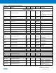
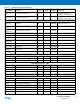
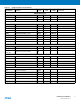
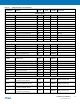
4.2 324-ball TFBGA Package Pinout Table 4-1.
Table 4-1.
Table 4-1.
5. Power Considerations 5.1 Power Supplies The SAM9M10 has several types of power supply pins: z VDDCORE pins: Power the core, including the processor, the embedded memories and the peripherals; voltage ranges from 0.9V to 1.1V, 1.0V typical. z VDDIOM0 pins: Power the DDR2/LPDDR I/O lines; voltage ranges between 1.65V and 1.95V (1.8V typical). z VDDIOM1 pins: Power the External Bus Interface 1 I/O lines; voltage ranges between 1.65V and 1.95V (1.8V typical) or between 3.0V and 3.6V (3.3V typical).
6. Processor and Architecture 6.
6.2 Bus Matrix z 12-layer Matrix, handling requests from 11 masters z Programmable Arbitration strategy z z z Fixed-priority Arbitration z Round-Robin Arbitration, either with no default master, last accessed default master or fixed default master Burst Management z Breaking with Slot Cycle Limit Support z Undefined Burst Length Support One Address Decoder provided per Master z z z 6.2.
6.2.2 Matrix Slaves Each Slave has its own arbiter, thus allowing a different arbitration per Slave to be programmed. Table 6-2. List of Bus Matrix Slaves Slave 0 Internal SRAM Internal ROM USB OHCI USB EHCI Slave 1 UDP High Speed RAM LCD User Interface Video Decoder 6.2.3 Slave 2 DDR Port 0 Slave 3 DDR Port 1 Slave 4 DDR Port 2 Slave 5 DDR Port 3 Slave 6 External Bus Interface Slave 7 Internal Peripherals Masters to Slaves Access All the Masters can normally access all the Slaves.
Figure 6-1. Video Mode Configuration D C N ideo Decoder LCD Post Processing DMA DDR S0 ARM I DDR S1 ARM I ARM D ARM D D C N DDR S2 MATRI DDR S3 Table 6-3. SAM9M10 Masters to Slaves Access with VDEC_SEL = 0 Master 0 1 2 3 4&5 6 7 8 9 10 11 ARM 926 Instr.
Table 6-4. SAM9M10 Masters to Slaves Access with VDEC_SEL = 1 (default) Master 0 1 2 3 4&5 6 7 8 9 10 11 ARM 926 Instr. ARM 926 Data PDC USB HOST OHCI DMA ISI DMA LCD DMA Ethern et MAC USB Device HS USB Host EHCI VDEC Internal SRAM 0 X X X X X X - X X X - Internal ROM X X X - - - - - X - - UHP OHCI X X - - - - - - - - - UHP EHCI X X - - - - - - - - - LCD User Int.
Table 6-6. 6.4 Peripheral DMA Controller Instance name Channel T/R SPI0 Transmit SSC1 Transmit SSC0 Transmit TSADCC Receive DBGU Receive USART3 Receive USART2 Receive USART1 Receive USART0 Receive AC97C Receive SPI1 Receive SPI0 Receive SSC1 Receive SSC0 Receive USB The SAM9M10 features USB communication ports as follows: z 2 Ports USB Host full speed OHCI and High speed EHCI z 1 Device High speed USB Host Port A is directly connected to the first UTMI transceiver.
z memory to memory transfer z Peripheral to memory z Memory to peripheral The DMA controller can handle the transfer between peripherals and memory and so receives the triggers from the peripherals below. The hardware interface numbers are also given below in Table Table 6-7. 6.
7. Memories Figure 7-1.
7.1 Memory Mapping A first level of address decoding is performed by the AHB Bus Matrix, i.e., the implementation of the Advanced High performance Bus (AHB) for its Master and Slave interfaces with additional features. Decoding breaks up the 4 Gbytes of address space into 16 banks of 256 Mbytes. The banks 1 to 6 are directed to the EBI that associates these banks to the external chip selects NCS0 to NCS5.
z Internal SRAM C is only accessible by all the AHB Masters. After reset and until the Remap Command is performed, this SRAM block is accessible through the AHB bus at address 0x0030 0000 by all the AHB Masters. After Remap, this SRAM block also becomes accessible through the AHB bus at address 0x0 by the ARM926 Instruction and the ARM926 Data Masters. Within the 64 Kbyte SRAM size available, the amount of memory assigned to each block is software programmable according to Table 7-1. Table 7-1. 7.2.
z SAM-BA Boot in case no valid program is detected in external NVM, supporting z Serial communication on a DBGU z USB Device HS Port 7.2.4.2 BMS = 0, boot on external memory z Boot on on-chip RC z Boot with the default configuration for the Static Memory Controller, byte select mode, 16-bit data bus, Read/Write controlled by Chip Select, allows boot on 16-bit non-volatile memory. For optimization purpose, nothing else is done.
z Static Memory Controller z DDR2/SDRAM Controller z SLC Nand Flash ECC Controller z Additional logic for NAND Flash and CompactFlashTM z Optional Full 32-bit External Data Bus z Up to 26-bit Address Bus (up to 64MBytes linear per chip select) z Up to 6 chip selects, Configurable Assignment: z Static Memory Controller on NCS0 z DDR2/SDRAM Controller (SDCS) or Static Memory Controller on NCS1 z Static Memory Controller on NCS2 z Static Memory Controller on NCS3, Optional NAND Flash suppor
7.3.2.3 NAND Flash Error Corrected Code Controller z Tracking the accesses to a NAND Flash device by triggering on the corresponding chip select z Single bit error correction and 2-bit Random detection.
8. System Controller The System Controller is a set of peripherals that allows handling of key elements of the system, such as power, resets, clocks, time, interrupts, watchdog, etc. The System Controller User Interface also embeds the registers that configure the Matrix and a set of registers for the chip configuration. The chip configuration registers configure the EBI chip select assignment and voltage range for external memories. 8.
8.2 System Controller Block Diagram Figure 8-1. SAM9M10 System Controller Block Diagram System Controller VDDCO REPowered irq0-irq2 fiq periph_irq 2..
8.3 Reset Controller The Reset Controller is based on two Power-on-Reset cells, one on VDDBU and one on VDDCORE. The Reset Controller is capable to return to the software the source of the last reset, either a general reset (VDDBU rising), a wake-up reset (VDDCORE rising), a software reset, a user reset or a watchdog reset. The Reset Controller controls the internal resets of the system and the NRST pin output.
8.6 Slow Clock Selection The SAM9M10 slow clock can be generated either by an external 32768Hz crystal or the on-chip RC oscillator. The 32768 Hz crystal oscillator can be bypassed, by setting the bit OSC32BYP, to accept an external slow clock on XIN32. The internal RC oscillator and the 32768 Hz oscillator can be enabled by setting to 1 respectively RCEN bit and OSC32EN bit in the system controller user interface. OSCSEL command selects the slow clock source.
8.7 z Wait internal RC Startup Time for clock stabilization (software loop). z Switch from 32768 Hz oscillator to internal RC oscillator by setting the bit OSCSEL to 0. z Wait 5 slow clock cycles for internal resynchronization. z Disable the 32768Hz oscillator by setting the bit OSC32EN to 0. Power Management Controller The Power Management Controller provides all the clock signals to the system.
Figure 8-4. SAM9M10 Power Management Controller Block Diagram PLLACK USBS UHP48M USBDIV+1 USB OHCI UHP12M /4 USB EHCI /1,/2 PCK Processor Clock Controller UPLLCK int Divider MAINCK SLCK Prescaler /1,/2,/4,.../64 X /1 /1.5 /2 SysClk DDR /1 /2 MCK /3 /4 Peripherals Clock Controller ON/OFF Master Clock Controller SLCK MAINCK periph_clk[..] ON/OFF Prescaler /1,/2,/4,...,/64 pck[..] UPLLCK Programmable Clock Controller 8.7.
8.8 8.9 8.
z z One 32-bit Vector Register per interrupt source z Interrupt Vector Register reads the corresponding current Interrupt Vector Protect Mode z z Fast Forcing z 8.
9. Peripherals 9.1 Peripheral Mapping As shown in Figure 7-1, the Peripherals are mapped in the upper 256 Mbytes of the address space between the addresses 0xFFF7 8000 and 0xFFFC FFFF. Each User Peripheral is allocated 16K bytes of address space. 9.2 Peripheral Identifiers Table 9-1 defines the Peripheral Identifiers of the SAM9M10.
9.3 Peripheral Interrupts and Clock Control 9.3.1 System Interrupt The System Interrupt in Source 1 is the wired-OR of the interrupt signals coming from: z the DDR2/LPDDR Controller z the Debug Unit z the Periodic Interval Timer z the Real-Time Timer z the Real-Time Clock z the Watchdog Timer z the Reset Controller z the Power Management Controller The clock of these peripherals cannot be deactivated and Peripheral ID 1 can only be used within the Advanced Interrupt Controller. 9.3.
9.4.1 PIO Controller A Multiplexing Table 9-2.
9.4.2 PIO Controller B Multiplexing Table 9-3.
9.4.3 PIO Controller C Multiplexing Table 9-4.
9.4.4 PIO Controller D Multiplexing Table 9-5.
9.4.5 PIO Controller E Multiplexing Table 9-6.
10. Embedded Peripherals 10.1 Serial Peripheral Interface (SPI) z z z 10.2 10.
z RS485 with driver control signal z ISO7816, T = 0 or T = 1 Protocols for interfacing with smart cards z z IrDA modulation and demodulation z Test Modes z z 10.4 10.5 Communication at up to 115.2 Kbps Remote Loopback, Local Loopback, Automatic Echo Serial Synchronous Controller (SSC) z Provides serial synchronous communication links used in audio and telecom applications (with CODECs in Master or Slave Modes, I2S, TDM Buses, Magnetic Card Reader,...
10.7 Pulse Width Modulation Controller (PWM) z Four channels, one 16-bit counter per channel z Common clock generator, providing Thirteen Different Clocks z 10.8 10.
z 4-bit single scan, 8-bit single or dual scan, 16-bit dual scan STN interfaces supported z Up to 24-bit single scan TFT interfaces supported z Up to 16 gray levels for mono STN and up to 4096 colors for color STN displays z 1, 2 bits per pixel (palletized), 4 bits per pixel (non-palletized) for mono STN z 1, 2, 4, 8 bits per pixel (palletized), 16 bits per pixel (non-palletized) for color STN z 1, 2, 4, 8 bits per pixel (palletized), 16, 24 bits per pixel (non-palletized) for TFT z Single cloc
z Vertical and horizontal resolutions up to 2048 x 2048 z Preview Path up to 640*480 z Support for packed data formatting for YCbCr 4:2:2 formats z Preview scaler to generate smaller size image 10.
z H.263 Profile 0, levels 10-70 z VC-1 z Simple Profile, Low and Medium Levels z Main Profile, Low, Medium and High Levels z Advanced Profile, Levels 0-3 z MPEG-2 Main Profile, Low, Medium and High Levels z JPEG Profile Baseline DCT (sequential) and JFIF 1.02 file form Post-processor features: z Image up-scaling z Image down-scaling z YCbCr to RGB conversion z Dithering z Deinterlacing z Programmable alpha channel z Alpha blending z De-blocking filter for MPEG-4 simple profile/H.
11. Mechanical Characteristics 11.1 Package Drawings Figure 11-1.
Table 11-1. Soldering Information Ball Land 0.4 mm +/- 0.05 Soldering Mask Opening 0.275 mm +/- 0.03 Table 11-2. Device and 324-ball TFBGA Package Maximum Weight 400 mg Table 11-3. 324-ball TFBGA Package Characteristics Moisture Sensitivity Level 3 Table 11-4. Package Reference JEDEC Drawing Reference MO-210 JESD97 Classification e1 This package respects the recommendations of the NEMI User Group. 11.2 Soldering Profile Table 11-5 gives the recommended soldering profile from J-STD-020C.
11.3 Marking All devices are marked with the Atmel logo and the ordering code.
12. SAM9M10 Ordering Information Table 12-1.
Revision History In the tables that follow, the most recent version appears first. The initials “rfo” indicate changes requested by product experts, or made during proof reading as part of the approval process. Table 12-2. Doc. Rev Change Request Ref. Comments Product Overview: 6355ES Section 1. “Features”, under “Peripherals” , added DBGU to USART... rfo AT91 removed from SAM9M10 product name in headers, text and images.
Atmel Corporation 1600 Technology Drive Atmel Asia Limited Unit 01-5 & 16, 19F Atmel Munich GmbH Business Campus Atmel Japan G.K. 16F Shin-Osaki Kangyo Bldg San Jose, CA 95110 BEA Tower, Millennium City 5 Parkring 4 1-6-4 Osaki, Shinagawa-ku USA 418 Kwun Tong Road D-85748 Garching b. Munich Tokyo 141-0032 Tel: (+1) (408) 441-0311 Kwun Tong, Kowloon GERMANY JAPAN Fax: (+1) (408) 487-2600 HONG KONG Tel: (+49) 89-31970-0 Tel: (+81) (3) 6417-0300 www.atmel.