
User manual


Configuration
AT91SAM9M10-G45-EK User Guide 5-7
6495B–ATARM–21-Apr-10
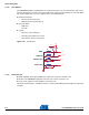
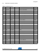
5.5.5 Multiplexing on PIO Controller D (PIOD)
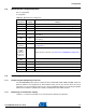
Table 5-7. PIO Multiplexing Port D
I/O Peripheral A Peripheral B Function and Comments Power
PD0 TK0 PWM3 Command LED2 VDDIOP0
PD1 TF0 Output ENA USB Host VDDIOP0
PD2 TD0 Input FLGA USB Host VDDIOP0
PD3 RD0 Output ENB USB Host VDDIOP0
PD4 RK0 Input FLGB USB Host VDDIOP0
PD5 RF0 Int. Ethernet 10/100 MDINTR VDDIOP0
PD6 AC97RX AC97 Receive Signal VDDIOP0
PD7 AC97TX TIOA5 AC97 Transmit Signal VDDIOP0
PD8 AC97FS TIOB5 AC97 Frame Sync Signal VDDIOP0
PD9 AC97CK TCLK5 AC97 Clock Signal VDDIOP0
PD10 TD1 Card Detect MMCI0 MCI0_CD VDDIOP0
PD11 RD1 Card Detect MMCI1 MCI1_CD VDDIOP0
PD12 TK1 PCK0 CTRL1 Image Sensor Interface VDDIOP0
PD13 RK1 CTRL2 Image Sensor Interface VDDIOP0
PD14 TF1 GPIO1 Large LCD (connector) VDDIOP0
PD15 RF1 GPIO2 Large LCD (connector) VDDIOP0
PD16 RTS1 USART1 Request to Send VDDIOP0
PD17 CTS1 USART1 Clear To Send VDDIOP0
PD18 SPI1_NPCS2 IRQ VDDIOP0
PD19 SPI1_NPCS3 FIQ VDDIOP0
PD20 TIOA0 TSAD0 Touch screen X_Right VDDANA
PD21 TIOA1 TSAD1 Touch screen X_Left VDDANA
PD22 TIOA2 TSAD2 Touch screen Y_Up VDDANA
PD23 TCLK0 TSAD3 Touch screen Y_Down VDDANA
PD24 SPI0_NPCS1 PWM0 GPAD4 General purpose A/D4 VDDANA
PD25 SPI0_NPCS2 PWM1 GPAD5 General purpose A/D5 VDDANA
PD26 PCK0 PWM2 GPAD6 General purpose A/D6 VDDIOP0
PD27 PCK1 SPI0_NPCS3 GPAD7 General purpose A/D7 VDDIOP0
PD28 TSADTRG SPI1_NPCS1 USB Plug-ID IDUSB VDDIOP0
PD29 TCLK1 SCK1 MCI1_WP VDDIOP0
PD30 TIOB0 SCK2 Command Power Led VDDIOP0
PD31 TIOB1 PWM1 Command LED1 VDDIOP0