AT91SAM9M10-G45-EK ....................................................................................................................
Section 1 Introduction .................................................................................................................1-1 1.1 Scope ................................................................................................................................. 1-1 1.2 Applicable Documents ....................................................................................................... 1-2 Section 2 Kit Contents ....................................................................
4.2.15 Expansion Slot ................................................................................................... 4-22 Section 5 Configuration ..............................................................................................................5-1 5.1 JTAG/ICE Configuration..................................................................................................... 5-1 5.2 ETHERNET Configuration ....................................................................................
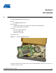
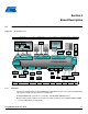
Section 1 Introduction 1.1 Scope This User Guide introduces the AT91SAM9M10(G45) Evaluation Kit and describes its development and debugging capabilities. Figure 1-1. Board Photo The Atmel® SAM9M10-G45-EK is a fully-featured evaluation platform for the Atmel AT91SAM9M10 or AT91SAM9G45 microcontroller. The kit is equipped with an AT91SAM9M10 chip, which is a superset of the AT91SAM9G45, and therefore allows evaluating that reference as well.
Introduction An LCD TFT display (480*272 RGB) with resistive touch panel A composite video output A camera interface Several communication peripherals such as: – Universal Synchronous/Asynchronous Receiver Transmitter (USART) – Two-Wire Interface (TWI) The external memory block is made of 3 memory types: 1.2 DDR2-SDRAM NAND Flash NOR Flash (not populated by default) Applicable Documents Table 1-1.
Section 2 Kit Contents 2.1 Deliverables The Atmel SAM9M10-G45-EK toolkit includes: Board – The SAM9M10-G45-EK board Power supply – Universal input AC/DC power supply with US, Europe and UK plug adapters – One 3V Lithium Battery type CR1225 Cables – One micro A/B-type USB cable – One serial RS232 cable – One RJ45 crossed cable A Welcome Letter Figure 2-1. Unpacked SAM9M10-G45-EK Unpack and inspect this kit carefully.
Kit Contents 2.2 Evaluation Board Specifications Table 2-1. SAM9M10-G45-EK Specifications 2.
Section 3 Power up 3.1 Power Up the Board Unpack the board taking care to avoid electrostatic discharge. Unpack the power supply, select the right power plug adapter corresponding to that of your country, and insert it in the power supply. Connect the power supply DC connector to the board and plug the power supply to an AC power plug. The board LCD should light up and display a welcome page. Then, click or touch icons displayed on the screen and enjoy the demo. 3.
Power up 3.4 Recovery Procedure The DevStart ends by giving step-by-step instructions on how to recover the SAM9M10-G45-EK to the state as it was when shipped by Atmel. Follow the instructions if you deleted the contents of the NAND Flash and want to recover from this situation. 3.5 Sample Code and Technical Support After boot up, you can run some sample code or your own application on the development kit. You can download sample code and get Technical support from http://www.atmel.
Section 4 Board Description 4.1 Equipment on the Board Figure 4-1. Board Architecture Main Memory Multimedia cards LCD TFT Data Flash PARALLEL FLASH NPCS0 4 bits interface SD/MMC Micro MCI1 MCI1 EBI1 / 1.8v EBI1 / 1.8v Touch Touch Screen Screen Joystick & P.
Board Description 4.1.2 4.1.3 One TWI serial memory One USB Host/Device multiplexed port interface One USB Host port interface One RS232 serial communication port One DBGU serial communication port One JTAG/ICE debug interface One Ethernet 100-base TX with three status LEDs One AC97 Audio CODEC with headphone line out, line in and mono/stereo microphone inputs One TV interface (composite video output) One 4.
Board Description Display LCD and LEDs Display, 480xRGBx272 pixels LCD module display connected to the PIO port E (LCD1) One surface-mounted power red LED, user interface (D3) Two surface-mounted green LEDs, user interface (D1 and D2) Three surface-mounted LEDs indicate Ethernet status (D4, D5, D6) Board Layout Commented 2 Y7 J15 TP1 C12 C9 C180 C181 C182 C27 C23 JP16 C6 BP2 WAKEUP JP12 L5 JP7 2 VDDBU BAT J3 3V J17 D1 BACKUP BATTERY D2 C31 R27 MN20 R183 R181 L20 TP6 R185
Board Description 4.2.2 Clock Circuitry The SAM9M10-G45-EK includes six clock sources: Two are alternatives for the SAM9M10 main clock, One crystal and one crystal oscillator are used for the Ethernet MII/RMII chip, One crystal is used for the AC97 codec chip, One crystal or one crystal oscillator is used for the TV encoder. Table 4-1. Main Components Associated with the Clock Systems Quantity 4.2.
AT91SAM9M10-G45-EK User Guide DDR_W E DDR_CAS DDR_RAS DDR_CS DDR_CLK DDR_NCLK DDR_CKE DDR_BA0 DDR_BA1 G7 F7 F3 CS CAS RAS NW E G1 L3 L7 E8 F8 G8 CK NCK F2 F9 G2 G3 H8 H3 H7 J2 J8 J3 J7 K2 K8 K3 H2 K7 L2 L8 CKE BA0 BA1 DDR_A0 DDR_A1 DDR_A2 DDR_A3 DDR_A4 DDR_A5 DDR_A6 DDR_A7 DDR_A8 DDR_A9 DDR_A10 DDR_A11 DDR_A12 DDR_A13 RFU1 RFU2 RFU3 WE CAS RAS CS CK CK CKE ODT BA0 BA1 A0 A1 A2 A3 A4 A5 A6 A7 A8 A9 A10 A11 A12 A13 MN6 DQS DQS DQ0 DQ1 DQ2 DQ3 DQ4 DQ5 DQ6 DQ7 VSSDL VSSQ VSSQ VSSQ
EBI1_FLASH_D[0..15] EBI1_DDR_D[0..
Board Description 4.2.5 Power Supplies The SAM9M10 Board contains four regulated power supplies: 3.3 VDC Supply 1.8 VDC Supply 1.0 VDC Core Supply 1.0 VDC Core UTMI Supply, PLL The outputs of these regulated power supplies1 are distributed as necessary to each part of the circuit board. The 3.3 VDC Supply is generated by an adjustable LDO. It accepts VIN 5 VCC power and outputs a regulated +3.3 V to most other circuits on the board. The 1.
Board Description Figure 4-5. Power Supply 3V3 J1-1 1 L1 2 VDDUTMII 10uH VDDANA R1 1R C1 100n C2 4.7u L2 10uH VDDOSC R5 1R C8 100n C14 4.7u JP1 1 3 JP2 VDDIOP0 2 1 3 JP3 VDDIOP1 2 1 3 2 VDDIOP2 VDDISI J1-2 3 1V_VDDUTMIC 4 VDDUTMIC 8 VDDPLLUTMI C15 2.2u R10 100k 3V3 J1-4 L3 10uH 7 R13 1 2 3 4 VIN VIN PGOOD EN EP MN3 RT9186A VOUT VOUT ADJ GND 8 7 6 5 1V_VDDUTMIC R14 12k C18 100n C19 C20 4.
Board Description Figure 4-6.
Board Description 4.2.6 Debug Interface 4.2.6.1 JTAG/ICE Software debug is accessed by a standard 20-pin JTAG connection. This allows connection to a standard USB-to-JTAG in-circuit emulator. Figure 4-7. JTAG Interface 5 6 7 8 3V3 3V3 3V3 RR43 100k 4 3 2 1 J13 2 4 6 8 10 12 14 16 18 20 1 3 5 7 9 11 13 15 17 19 R93 DNP R91 0R R92 0R 0R NTRST TDI TMS TCK RTCK TDO NRST NTRST TDI TMS TCK RTCK TDO NRST R94 0R DNP HTST-110-01-SM-D ICE INTERFACE 4.2.6.
Board Description 4.2.6.3 User Serial Com Port The USART1 is used as a user serial communication port. This USART1 is buffered with an RS-232 Transceiver (TXD, RXD and handshake CTS/RTS control) and connected to the DB-9 male socket. Software must assign the appropriate PIO pins (PB5 = RXD1, PB4 = TXD1, PD16 = RTS1, PD17 = CTS1) to enable the UART1 function.
Board Description Figure 4-10.
Board Description Table 4-2.
PA18 PA19 PD5 PA30 PA29 PA27 PA16 PA28 PA15 PA9 PA8 PA13 PA12 PA7 PA6 PA11 PA10 PA14 0R DNP R109 R110 R112 R114 (RX_CLK) (RX_DV) (TX_ER) (RX_ER) (COL) (CRS) (MDC) (MDIO) (MDINTR) 0R DNP 0R DNP R104 R105 (RXD3) (RXD2) (RXD1) (RXD0) NRST 0R DNP 0R DNP 0R DNP 0R DNP 0R DNP R108 R103 RR46 10k RR45 10k RR44 10k 3V3 8 7 6 5 1 2 3 4 (TXD3) (TXD2) (TXD1) (TXD0) (TX_EN) 8 7 6 5 1 2 3 4 (TX_CLK) 8 7 6 5 1 2 3 4 PA17 VDD 4 50MHz 2 VSS OUT 3 Y4 1 OE 10k JP16 3V3 R120 R122 0R 100
Board Description 4.2.7 Audio Stereo Interface The SAM9M10-G45-EK includes a WM9711L AC97 CODEC for digital sound input and output. This interface includes audio jacks for MIC input (J9), line audio input (J8), headphone line output (J7) and a 2-point speaker output connector (JP15). It is compliant with AC97 Component Specification V2.2.
Board Description Figure 4-12. Audio Stereo Interface HEADPHONE LINE-OUT 0R C126 R70 0R C127 + R69 100u/6.3V 1 2 + L6 220ohm at 100MHz 100u/6.3V 1 2 2 5 J7 JP17 DNP 2 1 JP18 DNP 2 1 100n 100n Y3 4 2 24.576MHz 22p C134 C135 10u 10V 100n C136 100n 1 C137 1 PD7 PD9 PD6 R78 AGND_AC97 1 2 3 4 5 6 7 8 9 10 11 12 49.
Board Description 4.2.8 TV-Out Extension The Chrontel™ CH7024 chip provides an interface between the SAM9M10 LCD Controller and a TV set by converting LCD signals to TV signals. The CH7024 is a TV encoder device which encodes the video signals and generates synchronization signals for NTSC and PAL standards. Supported TV output formats are NTSC-M, NTSC-J, NTSC-433, PAL-B/D/G/A/I, PAL-M, PAL-N and PAL-60. The CH7024 provides video output support for CVBS or Svideo. Figure 4-13. TV-Out Extension Port PE[0..
Board Description 4.2.9 Software Controlled LEDs Three users LED are provided for general use. The LEDs are connected to PIO port lines, allowing their control through either GPIO or PWM control. LEDs D1 to D3 are software controlled by PIO pins. LEDs D4 to D6 indicate Ethernet traffic and link status. These are automatically managed by on-chip microcontroller hardware. See Section 7.1 ”Schematics” . Table 4-3.
Board Description 4.2.10 Serial Peripheral Interface Controller (SPI) The SAM9M10 provides two high-speed Serial Peripheral Interface (SPI) controllers. One port is used to interface with the on-board serial DataFlash®. Figure 4-15. SPI 3V3 (test points) DNP JP11 PB0 PB1 PB2 PB3 R67 470k 3 1 2 (SPI0_MISO) (SPI0_MOSI) (SPI0_SPCK) (SPI0_NPCS0) 3V3 MN13 1 2 8 1 2 4 SO SI SCK CS 3 RESET JP12 SIP2 NRST VCC 6 GND 7 WP 5 C124 100n SERIAL DATAFLASH 4.2.
Board Description Figure 4-17. SD/MMC0 3V3 8 7 6 5 R191R192R193R194R195R196R197R198 RR36 10k 1 2 3 4 68k 68k 68k 68k 68k 68k 68k 68k (MCI1_W P) (MCI1_CD) PD29 PD11 PA[22..
Board Description Figure 4-19. TFT LCD (pinxx = display pin number ) 3V3 J24 1 2 3 4 5 6 7 8 9 10 11 12 13 14 15 16 17 18 19 20 21 22 23 24 25 26 27 28 29 30 31 32 33 34 35 36 37 38 39 40 41 42 43 44 45 Z7 LG PHILIPS 4.
Board Description 4.2.14 Push Buttons The SAM9M10-G45-EK is equipped with two system push buttons, two user push buttons and one joystick. The push buttons consist of momentary push button switches mounted directly to the board. When any switch is depressed, a low (zero) appears at the associated input pin.
Board Description Figure 4-21.
Section 5 Configuration 5.1 JTAG/ICE Configuration Table 5-1. JTAG/ICE Configuration Designation 5.2 Default Setting Feature R91 Not populated Disables the ICE NTRST input R92 Soldered Enables the ICE RTCK return. R94 must be opened R93 Soldered Enables the ICE NRST input R94 Not populated Disables TCK <-> RTCK local loop ETHERNET Configuration RMII is the factory default mode.
Configuration 5.3 Jumpers Configuration Two types of jumpers are used on the SAM9M10-G45-EK board: 2-pin jumpers with two possible settings: – Fitted: the circuit is closed – Not fitted: the circuit is open 3-pin jumpers with two possible positions, for which settings are presented in the following tables. Table 5-2.
Configuration 5.4 Miscellaneous Configuration Items N.P = not populated P = populated Table 5-3. Miscellaneous Configuration Designation Default Setting R34 N.P R35 P Connect TSADVREF to VDDANA (may be used for specific filtering) R36 P Connect GNDANA to GND (may be used for specific filtering) R38 P Force TST pin to GND (chip is set in non-test mode = normal operation mode) R63 N.P Write protect NAND Flash (mount a 0-ohm resistor to write-protect the NAND Flash device) R68 N.
Configuration Table 5-4.
Configuration 5.5.3 Multiplexing on PIO Controller B (PIOB) Table 5-5.
Configuration 5.5.4 Multiplexing on PIO Controller C (PIOC) Table 5-6.
Configuration 5.5.5 Multiplexing on PIO Controller D (PIOD) Table 5-7. PIO Multiplexing Port D I/O Peripheral A Peripheral B PD0 TK0 PWM3 PD1 Function and Comments Power Command LED2 VDDIOP0 TF0 Output ENA USB Host VDDIOP0 PD2 TD0 Input FLGA USB Host VDDIOP0 PD3 RD0 Output ENB USB Host VDDIOP0 PD4 RK0 Input FLGB USB Host VDDIOP0 PD5 RF0 Int.
Configuration 5.5.6 Multiplexing on PIO Controller E (PIOE) Table 5-8. PIO Multiplexing Port E I/O Peripheral A PE0 LCDPWR PE1 Peripheral B Power LCD Panel Pow.Enab.Ctrl VDDIOP1 LCDMOD LCD Modulation Signal VDDIOP1 PE2 LCDCC LCD Contrast Control VDDIOP1 PE3 LCDVSYNC LCD Vertical Synch. VDDIOP1 PE4 LCDHSYNC LCD Horizontal Synch.
Section 6 Connectors 6.1 Power Supply The SAM9M10-G45-EK evaluation board can be powered from a DC 5V power supply via the external power supply jack (J2) shown in Figure 6-1. The positive pole must be on J2 center pin. Figure 6-1. Power Supply Connector J2 Table 6-1. Power Supply Connector J2 Signal Description 6.2 Pin Mnemonic Signal description 1 Center +5 VCC 2 Gnd RS232 Connector with RTS/CTS Handshake Support Connector J11 is the COM1 connector. Figure 6-2.
Connectors Table 6-2. Serial COM1 Connector J11 Signal Descriptions Pin 1, 4, 6, 9 6.3 Mnemonic Signal description NC NO CONNECTION 2 TXD TRANSMITTED DATA RS232 serial data output signal 3 RXD RECEIVED DATA RS232 serial data input signal 5 GND GROUND 7 RTS READY TO SEND Active-positive RS232 input signal 8 CTS CLEAR TO SEND Active-positive RS232 output signal DBGU Connector J10 is the DBGU connector. Figure 6-3. RS232 DBGU Connector J10 Table 6-3.
Connectors 6.4 Ethernet Connector J15 is the RJ-45 Ethernet Connector. Figure 6-4. Ethernet RJ45 Connector J15 Table 6-4. Ethernet RJ45 Connector J15 Signal Descriptions Pin 6.5 Mnemonic Pin Mnemonic 1 TxData+ DIFFERENTIAL OUTPUT PLUS 2 Txdata- DIFFERENTIAL OUTPUT MINUS 3 RxData+ DIFFERENTIAL INPUT PLUS 4 Shield 5 Shield 6 RxData- DIFFERENTIAL INPUT MINUS 7 Shield 8 Shield USB Host Connector J12 is the USB Host connector. Figure 6-5. USB Host type A connector J12 Table 6-5.
Connectors 6.6 USB Host/Device Connector J14 is the USB Host/Device connector. Figure 6-6. USB Host/Device Micro AB connector J14 Table 6-6. USB Host/Device MicroAB Connector J14 Signal Descriptions Pin 6.7 Mnemonic Signal description 1 Vbus 5v power 2 DM Data minus 3 DP Data plus 4 ID On the Go Identification 5 Gnd Ground JTAG Debugging Connector Connector J13 is the JTAG/ICE connector. A SAM-ICE connector is a 20-way Insulation Displacement Connector (IDC) keyed box header (2.
Connectors Table 6-7. JTAG/ICE Connector J13 Signal Descriptions Pin Mnemonic Description 1 VTref. 3.3V power This is the target reference voltage. It is used to check if the target has power, to create the logic-level reference for the input comparators, and to control the output logic levels to the target. It is normally fed from VDD on the target board and must not have a series resistor. 2 Vsupply. 3.3V power This pin is not connected in SAM-ICE.
Connectors 6.8 SD/MMC- MCI0 Connector J6 is the SD/MMC connector. Figure 6-8. SD/MMC0 Connector J6 Table 6-8.
Connectors 6.9 SD/MMC- MCI1 Connector J5 is the SD/MMC connector. Figure 6-9. SD/MMC1 Connector J5 Table 6-9.
Connectors 6.10 AC97 Connector J7 is the Headphone connector. Connector J8 is the Line In connector. Connector J9 is the Microphone Input. Connector JP15 is the Speaker Output connector Figure 6-10. Audio Connector J7, J8, J9 Table 6-10. J7, J8, J9 Signal Description Pin Mnemonic 1 Signal 2 Signal 3 Gnd Table 6-11.
Connectors 6.11 Image Sensor - ISI Connector J17 is the ISI connector. Figure 6-11. ISI Connector J17 Table 6-12.
Connectors 6.12 Video Connector J20 is the Video connector Figure 6-12. Video Connector J20 Table 6-13. Video Connector J20 Signal Description Pin Mnemonic Signal description 1 Center Composite video signal output 6.13 Display Devices 6.13.1 TFT LCD Connector J24 is the TFT-LCD connector. Figure 6-13. TFT LCD Connector J24 Table 6-14.
Connectors Table 6-14. TFT LCD Connector J24 Signal Descriptions 6.14 Pin Mnemonic Pin Mnemonic 11 R6 12 R7 13 G0 14 G1 15 G2 16 G3 17 G4 18 G5 19 G6 20 G7 21 B0 14 B1 23 B2 16 B3 25 B4 18 B5 27 B6 20 B7 29 GND 30 DCLK 31 DISPON 32 HSYNC 33 VSYNC 34 LCDEN 35 NO CONNECT 36 GND 37 X2 38 Y1 39 X1 40 Y2 LCD Extension Connectors J23 and J18 are for an optional LCD extension (not populated). Table 6-15.
Connectors Table 6-15. Connector J23 Signal Description for an LCD Extension Pin Mnemonic Pin Mnemonic 31 PE6 LCDDEN 32 PE2 LCDCC 33 PE0 DISPON 34 PE1 LCDMOD 35 PD14 GPIO1 36 PD15 GPIO2 37 GND (0V) 38 GND (0V) 39 VCC +3V3 power source 40 NC Table 6-16.
Section 7 Schematics 7.
7 6 4 3 2 1 3V3 POWER SUPPLY 1V8 POWER USER INTERFACE D 5 EBI0 EBI0 DDR2 INTERFACE 1V DDR2 128MB 5V 8 EBI0 DDR2 INTERFACE PIO D Sheet 2 EBI1 DDR2 INTERFACE HOST EBI1 DATA INTERFACE ICE INTERFACE PIO A,...E ATMEL ARM9 Processor SAM9M10 (LFBGA324) 10/100 FAST ETHERNET RJ 45 EBI1 NANDFLASH INTERFACE EBI1 BUS INTERFACE Sheet 9 C EBI1 FLASH INTERFACE EBI1 ADDRESS INTERFACE FLASH HOST DEVICE NAND FLASH PIO Sheet 6 Sheet 4 PIO CARD READER PIO A,...
8 7 6 5 4 3 2 1 3V3 J1-1 1 1V C4 33u CR1 5V + DC POWER JACK C9 10u PGOOD EN VIN VDD C10 1u GND ADJ VOUT NC 8 7 6 5 C3 10n R4 47k 1 2 3 4 R199 3V3 MN1 RT9186A VIN VIN PGOOD EN 100k EP 1 2 3 4 MN2 RT9018A VOUT VOUT ADJ GND 8 7 6 5 L2 C5 10n R6 12k R7 15k C11 1u C13 1u C12 10u 10uH C7 1u R8 47k C8 100n C14 4.7u JP1 1 3 2 JP2 1 VOUT = 0.
{4} EBI0_CKE {4} EBI0_CLK {4} EBI0_NCLK {4} EBI0_CS {4} EBI0_CAS {4} EBI0_RAS {4} EBI0_WE {5,6} DDR_VREF {4} EBI0_DQM0 {4} EBI0_DQM1 {4} EBI0_DQS0 {4} EBI0_DQS1 G17 G16 J16 J18 H18 H14 H17 J17 H15 A16 G14 H16 G18 G15 EBI0_DDR_BA0 EBI0_DDR_BA1 EBI0_DDR_CKE EBI0_DDR_CLK EBI0_DDR_NCLK EBI0_DDR_CS EBI0_DDR_CAS EBI0_DDR_RAS EBI0_DDR_W E EBI1_DQM0 EBI1_DQM1 EBI1_DQS0 EBI1_DQS1 EBI1_RAS EBI1_CAS EBI1_SDW E EBI1_SDA10 EBI1_SDCKE EBI1_NCS0 EBI1_NCS1/SDCS EBI0_DDR_DQM0 EBI0_DDR_DQM1 EBI1_NRD/CFOE EBI1_NW E/NW R
8 7 6 5 4 EBI Bus Impedance Adaptor EBI1_D0 4 RR1D 5 3 2 EBI1_DDR_D[0..15] EBI1_DDR_D0 {3} EBI1_D[0..15] DDR_D[0..15] {3} EBI0_D[0..
8 D 7 6 5 4 3 2 1 {4} DDR_D[0..15] D {4} DDR_A[0..
8 7 6 5 4 3 2 1 {4} EBI1_FLASH_D[0..15] {4} EBI1_FLASH_A[1..21] {4} EBI1_DDR_D[0..15] {4} EBI1_DDR_A[2..
8 7 6 5 4 3 2 1 3V3 3V3 R187R188R189R190 R64 10k D R65 10k R191R192R193R194R195R196R197R198 8 7 6 5 D 68k 68k 68k 68k RR36 10k 1 2 3 4 68k 68k 68k 68k 68k 68k 68k 68k RR38 27R 1 8 2 7 3 6 4 5 PA3 PA2 (MCI0_DA1) (MCI0_DA0) PA0 (MCI0_CK) PA1 PA5 PA4 (MCI0_CDA) (MCI0_DA3) (MCI0_DA2) 1 2 3 4 8 7 6 5 RR40 27R 3V3 8 7 C122 100n 6 5 4 3 2 1 9 J6 (MCI1_W P) (MCI1_CD) {3} PD29 {3} PD11 {3,10} PA[22..31] (MCI0_CD) {3} PD10 {3} PA[0..
8 7 6 5 4 3 2 1 2 JP18 DNP 1 3V3 22p C137 22p C {3} PD7 {3} PD9 {3} PD6 100k AGND_AC97 MN14 Y3 4 24.576MHz (AC97TX) (AC97CK) C131 100n C134 10u 10V R78 C135 100n 1 2 3 4 5 6 7 8 9 10 11 12 49.
7 3V3 C158 SERIAL DEBUG PORT 1 6 2 7 3 8 4 9 5 D 100n 16 MN15 VCC 15 C157 J10 6 C165 GND 100n 2 C1C2+ V+ 100n 6 V- C2- 14 7 1 3 4 4 C160 100n C163 100n R87 100k 5 R89 100k R88 100k PB13 {3} R86 100k C164 100n PB12 {3} 3 4 5 V+ C2- V- RS232 COM PORT C161 100n 15 GND 2 C162 100n 6 C166 100n 7 T J11 1 6 2 7 3 8 4 9 5 14 T 12 D 13 10 R 10 {3} PB5 16 VCC C1C2+ 10 1 3V3 MN16 C1+ 11 {3} PB4 {3} PD16 12 R 2 1 3V3 10 T 3 3V3 C159 100n 11 T
8 7 6 5 4 3 2 1 3V3 D VDD 4 C173 100n {3} PA17 C {3} {3} {3} {3} {3} PA7 PA6 PA11 PA10 PA14 {3} {3} {3} {3} PA9 PA8 PA13 PA12 {3,7} PA28 {3} PA15 {3,7} PA27 {3} PA16 {3,7} PA30 {3,7} PA29 42 R101 0R R106 17 18 19 20 21 0R DNP 22 (TXD3) (TXD2) (TXD1) (TXD0) (TX_EN) R108 R103 0R DNP 0R DNP (RXD3) (RXD2) (RXD1) (RXD0) R104 R105 0R DNP 0R DNP 26 27 28 29 (RX_CLK) (RX_DV) R109 0R DNP 34 37 (TX_ER) (RX_ER) R110 0R DNP 16 38 (COL) (CRS) R112 R114 0R DNP 0R DNP 3V3 (MDC) (M
8 7 6 5 4 3 2 1 J24 M1 40 39 38 37 36 35 34 33 32 31 30 29 28 27 26 25 24 23 22 21 20 19 18 17 16 15 14 13 12 11 10 9 8 7 6 5 4 3 2 1 D TRULY 4.
8 7 6 5 4 3 2 1 CONNECTOR EXTENSION FOR LARGE LCD {3,11} PE[0..30] 1 {2,3,7,8,9,10} PE6 21 22 23 NRST 24 3V3 AVDD AGND AVDD_DAC AGND_DAC V H XCLK DE ISET CVBS 10k DNP Y6 1 OE VDD 4 Y SPD SPC C/CVBS RESET NC 34 R184 2 VSS B AGND_PLL 4.7k 4.
Section 8 Revision History 8.1 Revision History Table 8-1. Document 6495B 6495A Comments Change Request Ref. Main edits: - Most Figures updated - Hyperlinks to PDFs updated - ‘Serial Synchronous Controller (SSC)’ removed - ‘JTAG’ added - ‘RJ45 crossed cable’ added - Dimensions updated - Most configuration tables (with LEDs, pins and connectors) updated - ‘LG/Philips’ reference removed 6990 New Figure 4-4, ” EBI1 - DDR2 + Flash” and new Schematics in Section 7.1 ”Schematics” 7169 First issue.
Headquarters International Atmel Corporation 2325 Orchard Parkway San Jose, CA 95131 USA Tel: 1(408) 441-0311 Fax: 1(408) 487-2600 Atmel Asia Unit 1-5 & 16, 19/F BEA Tower, Millennium City 5 418 Kwun Tong Road Kwun Tong, Kowloon Hong Kong Tel: (852) 2245-6100 Fax: (852) 2722-1369 Atmel Europe Le Krebs 8, Rue Jean-Pierre Timbaud BP 309 78054 Saint-Quentin-enYvelines Cedex France Tel: (33) 1-30-60-70-00 Fax: (33) 1-30-60-71-11 Atmel Japan 9F, Tonetsu Shinkawa Bldg.