
Datasheet


812
SAM9M10 [DATASHEET]
6355F–ATARM–12-Mar-13
38.6 USB High Speed Device Port (UDPHS) User Interface
Notes: 1. The reset value for UDPHS_EPTCTL0 is 0x0000_0001.
2. The addresses for the UDPHS Endpoint registers shown here are for UDPHS Endpoint0. The structure of this group of reg-
isters is repeated successively for each endpoint according to the consecution of endpoint registers located between 0x120
and 0x1DC.
3. The addresses for the UDPHS DMA registers shown here are for UDPHS DMA Channel1. (There is no Channel0) The
structure of this group of registers is repeated successively for each DMA channel according to the consecution of DMA reg-
isters located between 0x320 and 0x370.
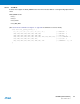
Table 38-5. Register Mapping
Offset Register Name Access Reset
0x00 UDPHS Control Register UDPHS_CTRL Read-write 0x0000_0200
0x04 UDPHS Frame Number Register UDPHS_FNUM Read 0x0000_0000
0x08 - 0x0C Reserved – – –
0x10 UDPHS Interrupt Enable Register UDPHS_IEN Read-write 0x0000_0010
0x14 UDPHS Interrupt Status Register UDPHS_INTSTA Read 0x0000_0000
0x18 UDPHS Clear Interrupt Register UDPHS_CLRINT Write –
0x1C UDPHS Endpoints Reset Register UDPHS_EPTRST Write –
0x20 - 0xCC Reserved – – –
0xE0 UDPHS Test Register UDPHS_TST Read-write 0x0000_0000
0xE4 - 0xE8 Reserved – – –
0xF0 UDPHS Name1 Register UDPHS_IPNAME1 Read 0x4855_5342
0xF4 UDPHS Name2 Register UDPHS_IPNAME2 Read 0x3244_4556
0xF8 UDPHS Features Register UDPHS_IPFEATURES Read
0x100 + endpoint * 0x20 + 0x00 UDPHS Endpoint Configuration Register UDPHS_EPTCFG Read-write 0x0000_0000
0x100 + endpoint * 0x20 + 0x04 UDPHS Endpoint Control Enable Register UDPHS_EPTCTLENB Write –
0x100 + endpoint * 0x20 + 0x08 UDPHS Endpoint Control Disable Register UDPHS_EPTCTLDIS Write –
0x100 + endpoint * 0x20 + 0x0C UDPHS Endpoint Control Register UDPHS_EPTCTL Read 0x0000_0000
(1)
0x100 + endpoint * 0x20 + 0x10 Reserved (for endpoint) – – –
0x100 + endpoint * 0x20 + 0x14 UDPHS Endpoint Set Status Register UDPHS_EPTSETSTA Write –
0x100 + endpoint * 0x20 + 0x18 UDPHS Endpoint Clear Status Register UDPHS_EPTCLRSTA Write –
0x100 + endpoint * 0x20 + 0x1C UDPHS Endpoint Status Register UDPHS_EPTSTA Read 0x0000_0040
0x120 - 0x1DC UDPHS Endpoint1 to 6
(2)
Registers
0x1E0 - 0x300 Reserved
0x300 - 0x30C Reserved – – –
0x310 + channel * 0x10 + 0x00 UDPHS DMA Next Descriptor Address Register UDPHS_DMANXTDSC Read-write 0x0000_0000
0x310 + channel * 0x10 + 0x04 UDPHS DMA Channel Address Register UDPHS_DMAADDRESS Read-write 0x0000_0000
0x310 + channel * 0x10 + 0x08 UDPHS DMA Channel Control Register UDPHS_DMACONTROL Read-write 0x0000_0000
0x310 + channel * 0x10 + 0x0C UDPHS DMA Channel Status Register UDPHS_DMASTATUS Read-write 0x0000_0000
0x320 - 0x370 DMA Channel2 to 5
(3)
Registers