
Datasheet


669
SAM9M10 [DATASHEET]
6355F–ATARM–12-Mar-13
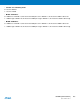
35.4 Application Block Diagram
Figure 35-2. Application Block Diagram
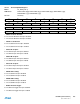
35.5 Pin Name List
Notes: 1. I: Input, O: Output, PP: Push/Pull, OD: Open Drain.
2. When several HSMCI (x HSMCI) are embedded in a product, MCCK refers to HSMCIx_CK, MCCDA to HSMCIx_CDA,
MCDAy to HSMCIx_DAy.
2345617
MMC
23456178
SDCard
9
Physical Layer
HSMCI Interface
Application Layer
ex: File System, Audio, Security, etc.
91011 12138
Table 35-1. I/O Lines Description
Pin Name
(2)
Pin Description Type
(1)
Comments
MCCDA Command/response I/O/PP/OD CMD of an MMC or SDCard/SDIO
MCCK Clock I/O CLK of an MMC or SD Card/SDIO
MCDA0 - MCDA7 Data 0..7 of Slot A I/O/PP DAT[0..7] of an MMC
DAT[0..3] of an SD Card/SDIO