
Datasheet


194
SAM9M10 [DATASHEET]
6355F–ATARM–12-Mar-13
• NRD_PULSE, NCS_RD_PULSE, NWE_PULSE, NCS_WR_PULSE
The SMC_CYCLE register groups the definition of all cycle parameters:
• NRD_CYCLE, NWE_CYCLE
Table 21-4 shows how the timing parameters are coded and their permitted range.
21.8.6 Reset Values of Timing Parameters
Table 21-8 gives the default value of timing parameters at reset.
21.8.7 Usage Restriction
The SMC does not check the validity of the user-programmed parameters. If the sum of SETUP and PULSE
parameters is larger than the corresponding CYCLE parameter, this leads to unpredictable behavior of the SMC.
For read operations:
Null but positive setup and hold of address and NRD and/or NCS can not be guaranteed at the memory interface
because of the propagation delay of theses signals through external logic and pads. If positive setup and hold val-
ues must be verified, then it is strictly recommended to program non-null values so as to cover possible skews
between address, NCS and NRD signals.
For write operations:
If a null hold value is programmed on NWE, the SMC can guarantee a positive hold of address, byte select lines,
and NCS signal after the rising edge of NWE. This is true for WRITE_MODE = 1 only. See “Early Read Wait State”
on page 195.
For read and write operations: a null value for pulse parameters is forbidden and may lead to unpredictable
behavior.
In read and write cycles, the setup and hold time parameters are defined in reference to the address bus. For
external devices that require setup and hold time between NCS and NRD signals (read), or between NCS and
NWE signals (write), these setup and hold times must be converted into setup and hold times in reference to the
address bus.
21.9 Automatic Wait States
Under certain circumstances, the SMC automatically inserts idle cycles between accesses to avoid bus contention
or operation conflict.
21.9.1 Chip Select Wait States
The SMC always inserts an idle cycle between 2 transfers on separate chip selects. This idle cycle ensures that
there is no bus contention between the de-activation of one device and the activation of the next one.
During chip select wait state, all control lines are turned inactive: NBS0 to NBS3, NWR0 to NWR3, NCS[0..5], NRD
lines are all set to 1.
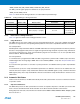
Table 21-4. Coding and Range of Timing Parameters
Coded Value Number of Bits Effective Value
Permitted Range
Coded Value Effective Value
setup [5:0] 6 128 x setup[5] + setup[4:0] 0 ≤ ≤ 31 0 ≤ ≤ 128+31
pulse [6:0] 7 256 x pulse[6] + pulse[5:0] 0 ≤ ≤ 63 0 ≤ ≤ 256+63
cycle [8:0] 9 256 x cycle[8:7] + cycle[6:0] 0 ≤ ≤ 127
0 ≤ ≤ 256+127
0 ≤ ≤ 512+127
0 ≤ ≤ 768+127