
Datasheet


193
SAM9M10 [DATASHEET]
6355F–ATARM–12-Mar-13
Figure 21-14. WRITE_MODE = 1. The write operation is controlled by NWE
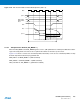
21.8.4.2 Write is Controlled by NCS (WRITE_MODE = 0)
Figure 21-15 shows the waveforms of a write operation with WRITE_MODE set to 0. The data is put on the bus
during the pulse and hold steps of the NCS signal. The internal data buffers are turned out after the
NCS_WR_SETUP time, and until the end of the write cycle, regardless of the programmed waveform on NWE.
Figure 21-15. WRITE_MODE = 0. The write operation is controlled by NCS
21.8.5 Coding Timing Parameters
All timing parameters are defined for one chip select and are grouped together in one SMC_REGISTER according
to their type.
The SMC_SETUP register groups the definition of all setup parameters:
• NRD_SETUP, NCS_RD_SETUP, NWE_SETUP, NCS_WR_SETUP
The SMC_PULSE register groups the definition of all pulse parameters:
MCK
D[31:0]
NCS
A
[25:2]
NBS0, NBS1,
NBS2, NBS3,
A0, A1
NWE,
NWR0, NWR1,
NWR2, NWR3
MCK
D[31:0]
NCS
NWE,
NWR0, NWR1,
NWR2, NWR3
A
[25:2]
NBS0, NBS1,
NBS2, NBS3,
A0, A1