
Datasheet


167
SAM9M10 [DATASHEET]
6355F–ATARM–12-Mar-13
Application Example
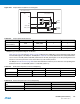
Figure 20-7 on page 167 illustrates an example of a CompactFlash application. CFCS0 and CFRNW signals are
not directly connected to the CompactFlash slot 0, but do control the direction and the output enable of the buffers
between the EBI and the CompactFlash Device. The timing of the CFCS0 signal is identical to the NCS4 signal.
Moreover, the CFRNW signal remains valid throughout the transfer, as does the address bus. The CompactFlash
_WAIT signal is connected to the NWAIT input of the Static Memory Controller. For details on these waveforms
and timings, refer to the Static Memory Controller Section.
Figure 20-7. CompactFlash Application Example
20.2.7.7 NAND Flash Support
External Bus Interfaces integrate circuitry that interfaces to NAND Flash devices.
External Bus Interface
The NAND Flash logic is driven by the Static Memory Controller on the NCS3 address space. Programming the
EBI_CS3A field in the EBI_CSA Register in the Chip Configuration User Interface to the appropriate value enables
NWR1/NBS1/CFIOR CFIOR NWR1/NBS1
NWR3/NBS3/CFIOW CFIOW NWR3/NBS3
A25/CFRNW CFRNW A25
Table 20-10. Shared CompactFlash Interface Multiplexing
Pins
Access to CompactFlash Device Access to Other EBI Devices
CompactFlash Signals EBI Signals
CompactFlash ConnectorEBI
D[15:0]
/OEDIR
_CD1
_CD2
/OE
D[15:0]
A25/CFRNW
NCS4/CFCS0
CD (PIO)
A[10:0]
A22/REG
NOE/CFOE
A[10:0]
_REG
_OE
_WE
_IORD
_IOWR
_CE1
_CE2
NWE/CFWE
NWR1/CFIOR
NWR3/CFIOW
CFCE1
CFCE2
_WAIT
NWAIT