
Datasheet


166
SAM9M10 [DATASHEET]
6355F–ATARM–12-Mar-13
Figure 20-6. CompactFlash Read/Write Control Signals
Multiplexing of CompactFlash Signals on EBI Pins
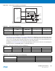
Table 20-9 on page 166 and Table 20-10 on page 166 illustrate the multiplexing of the CompactFlash logic signals
with other EBI signals on the EBI pins. The EBI pins in Table 20-9 are strictly dedicated to the CompactFlash inter-
face as soon as the EBI_CS4A and/or EBI_CS5A field of the EBI_CSA Register in the Chip Configuration User
Interface is set. These pins must not be used to drive any other memory devices.
The EBI pins in Table 20-10 on page 166 remain shared between all memory areas when the corresponding Com-
pactFlash interface is enabled (EBI_CS4A = 1 and/or EBI_CS5A = 1).
SMC
NRD_NOE
NWR0_NWE
A23
CFIOR
CFIOW
CFOE
CFWE
1
1
CompactFlash Logic
External Bus Interface
1
1
1
0
A22
1
0
1
0
1
0
Table 20-8. CompactFlash Mode Selection
Mode Base Address CFOE CFWE CFIOR CFIOW
Attribute Memory
Common Memory
NRD NWR0_NWE 1 1
I/O Mode 1 1 NRD NWR0_NWE
True IDE Mode 0 1 NRD NWR0_NWE
Table 20-9. Dedicated CompactFlash Interface Multiplexing
Pins
CompactFlash Signals EBI Signals
CS4A = 1 CS5A = 1 CS4A = 0 CS5A = 0
NCS4/CFCS0 CFCS0 NCS4
NCS5/CFCS1 CFCS1 NCS5
Table 20-10. Shared CompactFlash Interface Multiplexing
Pins
Access to CompactFlash Device Access to Other EBI Devices
CompactFlash Signals EBI Signals
NRD/CFOE CFOE NRD
NWR0/NWE/CFWE CFWE NWR0/NWE