
Datasheet


165
SAM9M10 [DATASHEET]
6355F–ATARM–12-Mar-13
The CFCE1 and CFCE2 waveforms are identical to the corresponding NCSx waveform. For details on these wave-
forms and timings, refer to the Static Memory Controller section.
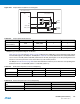
Read/Write Signals
In I/O mode and True IDE mode, the CompactFlash logic drives the read and write command signals of the SMC
on CFIOR and CFIOW signals, while the CFOE and CFWE signals are deactivated. Likewise, in common memory
mode and attribute memory mode, the SMC signals are driven on the CFOE and CFWE signals, while the CFIOR
and CFIOW are deactivated. Figure 20-6 on page 166 demonstrates a schematic representation of this logic.
Attribute memory mode, common memory mode and I/O mode are supported by setting the address setup and
hold time on the NCS4 (and/or NCS5) chip select to the appropriate values. For details on these signal waveforms,
please refer to the section: Setup and Hold Cycles of the Static Memory Controller section.
Table 20-7. CFCE1 and CFCE2 Truth Table
Mode CFCE2 CFCE1 DBW Comment SMC Access Mode
Attribute Memory NBS1 NBS0 16 bits Access to Even Byte on D[7:0] Byte Select
Common Memory
NBS1 NBS0 16bits
Access to Even Byte on D[7:0]
Access to Odd Byte on D[15:8]
Byte Select
1 0 8 bits Access to Odd Byte on D[7:0]
I/O Mode
NBS1 NBS0 16 bits
Access to Even Byte on D[7:0]
Access to Odd Byte on D[15:8]
Byte Select
1 0 8 bits Access to Odd Byte on D[7:0]
True IDE Mode
Task File 1 0 8 bits
Access to Even Byte on D[7:0]
Access to Odd Byte on D[7:0]
Data Register 1 0 16 bits
Access to Even Byte on D[7:0]
Access to Odd Byte on D[15:8]
Byte Select
Alternate True IDE Mode
Control Register
Alternate Status Read
01
Don’t
Care
Access to Even Byte on D[7:0] Don’t Care
Drive Address 0 1 8 bits Access to Odd Byte on D[7:0]
Standby Mode or
Address Space is not
assigned to CF
11– – –