
Datasheet


1322
SAM9M10 [DATASHEET]
6355F–ATARM–12-Mar-13
Notes: 1. Timings SSC4 and SSC7 depend on the start condition. When STTDLY = 0 (Receive start delay) and START = 4, or 5 or 7
(Receive Start Selection), two Periods of the MCK must be added to timings.
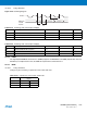
2. For output signals (TF, TD, RF), Min and Max access times are defined. The Min access time is the time between the TK (or
RK) edge and the signal change. The Max access time is the time between the TK edge and the signal stabilization. Figure
47-18 illustrates Min and Max accesses for SSC0. The same applies to SSC1, SSC4, and SSC7, SSC10 and SSC13.
Figure 47-18. Min and Max Access Time of Output Signals
47.15.3 ISI
47.15.3.1 Timing Conditions
Timings are given assuming capacitance loads on Table 47-38.
Receiver
SSC
8
RF/RD setup time before RK edge (RK input) 2.4 ns
SSC
9
RF/RD hold time after RK edge (RK input) t
CPMCK
ns
SSC
10
RK edge to RF (RK input) 5.4
(2)
21.5
(2)
ns
SSC
11
RF/RD setup time before RK edge (RK output) 18.6 - t
CPMCK
ns
SSC
12
RF/RD hold time after RK edge (RK output) t
CPMCK
- 5.1 ns
SSC
13
RK edge to RF (RK output) 0
(2)
5.3
(2)
ns
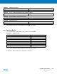
Table 47-37. SSC Timings with 1.8V Peripheral Supply (Continued)
Symbol Parameter Cond Min Max
Unit
s
TK (CKI =0)
TF/TD
SSC
0min
TK (CKI =1)
SSC
0max
Table 47-38. Capacitance Load
Corner
Supply MAX MIN
3.3V 30pF 0 pF
1.8V 20pF 0 pF