
Datasheet


1310
SAM9M10 [DATASHEET]
6355F–ATARM–12-Mar-13
– T1 = 66 μs
– T2 = 352 μs
In conclusion, establish VDDIOP and VDDIOM first, and VDDCORE last to ensure reliable operation of the device.
VDDOSC, VDDPLL, VDDUTMII and VDDUTMIC must be started at any time but before VDDCORE to ensure cor-
rect behavior of the ROM code.
47.13 SMC Timings
47.13.1 Timing Conditions
SMC Timings are given for MAX corners.
Timings are given assuming a capacitance load on data, control and address pads:
In the following tables, t
CPMCK
is MCK period.
47.13.2 Timing Extraction
47.13.2.1 Zero Hold Mode Restrictions
47.13.2.2 Read Timings
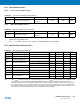
Table 47-26. Capacitance Load
Corner
Supply MAX MIN
3.3V 50pF 5 pF
1.8V 30 pF 5 pF
Table 47-27. Zero Hold Mode Use Maximum system clock frequency (MCK)
Symbol Parameter Min Units
VDDIOM supply 1.8V 3.3V
Zero Hold Mode Use
Fmax MCK frequency 66 66 MHz
Table 47-28. SMC Read Signals - NCS Controlled (READ_MODE= 1)
Symbol Parameter Min Units
VDDIOM supply 1.8V 3.3V
NO HOLD SETTINGS (nrd hold = 0)
SMC
1
Data Setup before NRD High 12.0 11.2 ns
SMC
2
Data Hold after NRD High 0 0 ns
HOLD SETTINGS (nrd hold ≠ 0)
SMC
3
Data Setup before NRD High 8.7 8.2 ns
SMC
4
Data Hold after NRD High 0 0 ns