
Datasheet


1308
SAM9M10 [DATASHEET]
6355F–ATARM–12-Mar-13
47.11 Touch Screen ADC (TSADC)
Note: 1. The Track-and-Hold Acquisition Time is given by:
The ADC internal clock is divided by 2 in order to generate a clock with a duty cycle of 75%. So the maximum conversion
time is give by:
The full speed is obtained for an input source impedance of < 50 Ohms maximum, or TTH = 500 ns.
In order to make the TSADC work properly, the SHTIM field in TSADCC Mode Register is to be calculated according to this
Track and Hold Acquisition Time, also called Sampled and Hold Time.
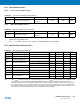
Table 47-21. Channel Conversion Time and ADC Clock
Parameter Conditions Min Typ Max Units
ADC Clock Frequency 10-bit resolution mode 13.2 MHz
Startup Time Return from Idle Mode 40 μs
Track and Hold Acquisition Time (TTH) ADC Clock = 13.2 MHz
(1)
0.5 μs
Conversion Time (TCT) ADC Clock = 13.2 MHz
(1)
1.75 μs
Throughput Rate ADC Clock = 13.2 MHz
(1)
440 kSPS
TTH (ns) 500 0.12 Z
IN
×()Ω()+=
TCT μs()
23
Fclk
---------- -
MHz()=
Table 47-22. External Voltage Reference Input
Parameter Conditions Min Typ Max Units
ADVREF Input Voltage Range 2.4 VDDANA V
ADVREF Average Current 600 μA
Current Consumption on VDDANA 300 μA
Table 47-23. Analog Inputs
Parameter Min Typ Max Units
Input Voltage Range 0 ADVREF V
Input Leakage Current 1μA
Input Capacitance 710pF
Input Source Impedance 50 Ohms
Table 47-24. Transfer Characteristics
Parameter Min Typ Max Units
Resolution 10 bit
Integral Non-linearity ±2 LSB
Differential Non-linearity -0.9 +0.9 LSB
Offset Error -1.5 0.5 ±10 mV
Gain Error ±2 LSB