
Datasheet


1306
SAM9M10 [DATASHEET]
6355F–ATARM–12-Mar-13
47.9 I/Os
Criteria used to define the maximum frequency of the I/Os:
• Output duty cycle (40%-60%)
• Minimum output swing: 100 mV to VDDIO - 100 mV
• Addition of rising and falling time inferior to 75% of the period
Notes: 1. V
VDDIOP
from 3.0V to 3.6V
2. V
VDDIOP
from 1.65V to 1.95V
47.10 USB HS Characteristics
47.10.1 Electrical Characteristics
47.10.2 Static Power Consumption
Note: 1. If cable is connected add 200 μA (Typical) due to Pull-up/Pull-down current consumption.
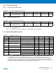
Table 47-17. I/O Characteristics
Symbol Parameter Conditions Min Max Units
FreqMax VDDIOP powered Pins frequency
3.3V domain
(1)
Max. external load = 20 pF
Max. external load = 40 pF
66
34
MHz
1.8V domain
(2)
Max. external load = 20 pF
Max. external load = 40 pF
35
18
MHz
Table 47-18. Electrical Parameters
Symbol Parameter Conditions Min Typ Max Unit
R
PUI
Bus Pull-up Resistor on
Upstream Port (idle bus)
in LS or FS Mode 1.5 kOhms
R
PUA
Bus Pull-up Resistor on
Upstream Port (upstream port
receiving)
in LS or FS Mode 15 kOhms
Setting time
T
BIAS
Bias settling time 20 μs
T
OSC
Oscillator settling time With Crystal 12MHz 2 ms
T
SETTLING
Settling time F
IN
= 12 MHz 0.3 0.5 ms
Table 47-19. Static Power Consumption
Symbol Parameter Conditions Min Typ Max Unit
I
BIAS
Bias current consumption on
VBG
1μA
I
VDDUTMII
HS Transceiver and I/O current
consumption
8μA
LS / FS Transceiver and I/O
current consumption
no connection(1) 3 μA
I
VDDUTMIC
Core, PLL, and Oscillator
current consumption
2 μA