
Datasheet


1301
SAM9M10 [DATASHEET]
6355F–ATARM–12-Mar-13
47.4 Clock Characteristics
47.4.1 Processor Clock Characteristics
47.4.2 Master Clock Characteristics
The master clock is the maximum clock at which the system is able to run. It is given by the smallest value of the
internal bus clock and EBI clock.
Note: 1. For DDR2 usage, there are no limitations to LDDDR, SDRAM and mobile SDRAM.
47.5 Main Oscillator Characteristics
Note: 1. The C
CRYSTAL
value is specified by the crystal manufacturer. In our case, C
CRYSTAL
must be between 15 pF and 20 pF. All par-
asitic capacitance, package and board, must be calculated in order to reach 15 pF (minimum targeted load for the
oscillator) by taking into account the internal load C
INT
. So, to target the minimum oscillator load of 15 pF, external capaci-
tance must be: 15 pF - 4 pF = 11 pF which means that 22 pF is the target value (22 pF from xin to gndosc and 22 pF from
xout to gndosc) If 20 pF load is targeted, the sum of pad, package, board and external capacitances must be 20 pF - 4 pF =
16 pF which means 32 pF (32 pF from xin to gndosc and 32 pF from xout to gndosc).
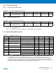
Table 47-5. Processor Clock Waveform Parameters
Symbol Parameter Conditions Min Max Units
1/(t
CPPCK
) Processor Clock Frequency
VDDCORE = 0.9V
T = 85°C
125
(1)
400 MHz
Table 47-6. Master Clock Waveform Parameters
Symbol Parameter Conditions Min Max Units
1/(t
CPMCK
) Master Clock Frequency
VDDCORE = 0.9V
T = 85°C
125
(1)
133 MHz
Table 47-7. Main Oscillator Characteristics
Symbol Parameter Conditions Min Typ Max Unit
1/(t
CPMAIN
) Crystal Oscillator Frequency 8 12 16 MHz
C
CRYSTAL
(1)
Crystal Load Capacitance 15 20 pF
C
INT
(1)
Internal Load Capacitance 4 pF
C
LEXT
External Load Capacitance
C
CRYSTAL
= 15 pF
(1)
22 pF
C
CRYSTAL
= 20 pF
(1)
32 pF
Duty Cycle 40 50 60 %
t
ST
Startup Time 2ms
I
DDST
Standby Current Consumption Standby mode 1 μA
P
ON
Drive Level 150 μW
I
DD ON
Current Dissipation
@ 8 MHz 0.35 0.55 mA
@ 16 MHz 0.7 1.1 mA