
Datasheet


966
SAM9G15 [DATASHEET]
11052D–ATARM–31-Oct-12
6. Enable the display power signal writing one to the DISPEN field of the LCDC_LCDEN register.
7. Poll DISPSTS field of the LCDC_LCDSR register to check that the power signal is activated.
The GUARDTIME field of the LCDC_LCDCFG5 register is used to configure the number of frames before the assertion
of the DISP signal.
44.6.1.4 Timing Engine Power Down Software Operation
The following sequence is used to disable the display:
1. Disable the DISP signal writing DISPDIS field of the LCDC_LCDDIS register.
2. Poll DISPSTS field of the LCDC_LCDSR register to verify that the DISP is no longer activated.
3. Disable the hsync and vsync signals by writing one to SYNCDIS field of the LCDC_LCDDIS register.
4. Poll LCDSTS field of the LCDC_LCDSR register to check that the synchronization is off.
5. Disable the Pixel clock by writing one in the CLKDIS field of the LCDC_LCDDIS register.
44.6.2 DMA Software Operations
44.6.2.1 DMA Channel Descriptor (DSCR) Alignment and Structure
The DMA Channel Descriptor (DSCR) must be word aligned.
The DMA Channel Descriptor structure contains three fields:
z DSCR.CHXADDR: Frame Buffer base address register
z DSCR.CHXCTRL: Transfer Control register
z DSCR.CHXNEXT: Next Descriptor Address register
44.6.2.2 Programming a DMA Channel
1. Check the status of the channel reading the CHXCHSR register.
2. Write the channel descriptor (DSCR) structure in the system memory by writing DSCR.CHXADDR Frame base
address, DSCR.CHXCTRL channel control and DSCR.CHXNEXT next descriptor location.
3. If more than one descriptor is expected, the DFETCH field of DSCR.CHXCTRL is set to one to enable the descrip-
tor fetch operation.
4. Write the DSCR.CHXNEXT register with the address location of the descriptor structure and set DFETCH field of
the DSCR.CHXCTRL register to one.
5. Enable the relevant channel by writing one to the CHEN field of the CHXCHER register.
6. An interrupt may be raised if unmasked when the descriptor has been loaded.
44.6.2.3 Disabling a DMA channel
1. Clear the DFETCH bit in the DSCR.CHXCTRL field of the DSCR structure will disable the channel at the end of the
frame.
2. Set the DSCR.CHXNEXT field of the DSCR structure will disable the channel at the end of the frame.
3. Writing one to the CHDIS field of the CHXCHDR register will disable the channel at the end of the frame.
4. Writing one to the CHRST field of the CHXCHDR register will disable the channel immediately. This may occur in
the middle of the image.
5. Poll CHSR field in the CHXCHSR register until the channel is successfully disabled.
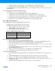
Table 44-4. DMA Channel Descriptor Structure
System Memory Structure Field for channel CHX
DSCR + 0x0 ADDR
DSCR + 0x4 CTRL
DSCR + 0x8 NEXT