
User manual
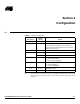
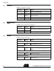
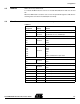

Table Of Contents
Configuration
4-2 AT91SAM9260-EK Evaluation Board User Guide
6234C–ATARM–22-Mar-07
4.2 JTAG/ICE
4.3 Microcontroller
Clock
4.4 Memory
Table 4-2. JTAG/ICE Configuration
Designation
Default
Setting Feature
S1 Opened Disables the ICE NTRST input
S2 Opened Selects ICE mode or JTAG mode (See Errata)
S3 Opened
Disables TCK <-> RTCK local loop. If S3 is closed, R13
must be unsoldered.
R13 Soldered Enables the ICE RTCK return. S3 must be opened
R14 Soldered Enables the ICE NRST input
Table 4-3. Microcontroller Clock Configuration
Designation
Default
Setting Feature
R18/R20 Soldered
Enables the use of 18.432MHz crystal. If external clock
used, R18/R20 must be unsoldered and S4 closed.
S4 Opened
J9 Slow Clock Setting. See
Table 4-1.
Table 4-4. Memory Configuration
Designation
Default
Setting Feature
SDRAM
R31
R32
Soldered
Soldered
Enables MN7 Chip select access
Enables MN8 Chip select access
NANDFlash (MN6x)
R36
R34
S6
Soldered
Soldered
Opened
Enables the use of NANDFlash (MN6x)
Enables the use of Ready Busy signalDisables write
protect
SERIAL DATAFLASH (MN9)
R40
S5
Soldered
Opened
Enable the use of the Serial DataFlash (MN9)
Disables the write protect.
TWI SERIAL EEPROM (MN10)
R46
R47
Soldered
Soldered
Enables SCL access
Enables SDA access