AT91SAM9260-EK Evaluation Board ..............................................................................................
AT91SAM9260-EK Evaluation Board User Guide 6234C–ATARM–22-Mar-07
Table of Contents Section 1 Overview ............................................................................................... 1-1 1.1 1.2 1.3 Scope ........................................................................................................1-1 Deliverables ..............................................................................................1-1 AT91SAM9260-EK Evaluation Board .......................................................
Table of Contents Section 5 Schematics ........................................................................................... 5-1 5.1 Schematics ...............................................................................................5-1 Section 6 Errata .................................................................................................... 6-1 6.1 6.2 6.3 VDD Backup Jumper Selector (J10) .........................................................6-1 JTAGSEL S2 Footprint Selector .
Section 1 Overview 1.1 Scope The AT91SAM9260-EK evaluation kit enables the evaluation of and code development for applications running on an AT91SAM9260 device. This guide focuses on the AT91SAM9260-EK board as an evaluation platform. The board supports the AT91SAM9260 in an LFBGA217 package as well as in a PQFP208 package. 1.
Overview ! one additional serial communication port with RTS/CTS handshake control ! JTAG/ICE debug interface ! one PHY Ethernet 100-base TX with three status LEDs ! one Atmel AT73C213 Audio DAC ! one Power LED and one general-purpose LED ! two user input push buttons ! one Wakeup input push button ! one reset push button ! one DataFlash, SD/MMC card slot ! four expansion connectors (PIOA, PIOB, PIOC, IMAGE SENSOR) ! one BGA-like EBI expansion footprint connector ! one Lithium Coin Cell Battery Retainer fo
Section 2 Setting Up the AT91SAM9260-EK Board 2.1 Electrostatic Warning The AT91SAM9260-EK evaluation board is shipped in protective anti-static packaging. The board must not be subjected to high electrostatic potentials. A grounding strap or similar protective device should be worn when handling the board. Avoid touching the component pins or any other metallic element. 2.
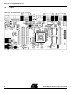
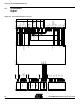
Setting Up the AT91SAM9260-EK Board 2.3 Layout Figure 2-1.
Setting Up the AT91SAM9260-EK Board Figure 2-2. AT91SAM9260-EK Layout - Bottom View 2.4 Powering Up the Board The AT91SAM9260-EK requires 5V DC (±5%). DC power is supplied to the board via the 2.1 mm by 5.5 mm socket J1. Coaxial plug center positive standard. 2.5 Backup Power Supply The user has the possibility to plug a battery (3V Lithium Battery CR1225 or equivalent) in order to permanently power the backup part of the device. In this case, J10 configuration must be set in position 1, 2.
5VDC AT73C213 TXD1 RXD1 RTS1 CTS1 COM0 COM1 PA[0..31] PB[0..
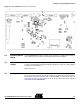
Section 3 Board Description 3.
Board Description Control • Clock Generator (CKGR) – Selectable 32768Hz Low-power Oscillator or Internal Low Power RC Oscillator on Battery Backup Power Supply, Providing a Permanent Slow Clock – 3 to 20 MHz On-chip Oscillator, One up to 240 MHz PLL and One up to 130 MHz PLL • Power Management Controller (PMC) – Very Slow Clock Operating Mode, Software Programmable Power Optimization Capabilities – Two Programmable External Clock Signals • Advanced Interrupt Controller (AIC) – Individually Maskable, Eight-
Board Description – High-Drive Capability on Ouputs TIOA0, TIOA1, TIOA2 • One Two-wire Interface (TWI) – Master, Multi-master and Slave Mode Operation – General Call Supported in Slave Mode – Connection to PDC Channel To Optimize Data Transfers in Master Mode Only • IEEE® 1149.1 JTAG Boundary Scan on All Digital Pins • Required Power Supplies: – 1.65V to 1.95V for VDDBU, VDDCORE, VDDOSC and VDDPLL – 3.0V to 3.
AIC DRXD DTXD PCK0-PCK1 DBGU In-Circuit Emulator I_ M IS CK I_ IS PC I_ K IS DO I_ -I V IS SY SI_ I_ N D7 HS C YN C HD HD PA M A HD PB HD M B IS 10/100 Ethernet MAC ARM926EJ-S Processor ICache 8 Kbytes DCache 8 Kbytes MMU FIFO I Image Sensor Interface USB OHCI DMA DMA D PLLB OSC WDT 6-layer Matrix 6 x 100M x 32-bit words PIT 4GPREG RC OSCSEL XIN32 XOUT32 OSC RTT PIOA SHDN WKUP VDDBU POR VDDCORE POR SHDC ROM 32 Kbytes PIOB Fast SRAM 4 Kbytes Fast SRAM 4 Kbytes Peripheral Bridg
Board Description 3.3 Microcontroller ! One LFBGA 217-ball fitted on board ! One LQFP 208-lead footprint To try the microcontroller in the LQFP package, the user has to unsolder MN4 and solder the PQFP208 microcontroller on the MN6 footprint. 3.4 Memory ! 32 Kbytes of Internal ROM ! Two 4-KByte Internal SRAM ! Atmel serial DataFlash ! 64 Mbytes of SDRAM memory (32-bit bus width) ! 256 Mbytes of NANDFlash memory (8-bit bus width) ! TWI serial EEPROM 3.5 Clock Circuitry ! 18.
Board Description 3.10 3.11 Audio Stereo Interface ! One Atmel stereo audio DAC (AT73C213) User Interface ! Two user input pushbuttons(2) ! One 32 Ohm/20 mW Stereo Headset output (J4) with master volume and mute controls ! One user green LED ! One yellow power LED (can be also software controlled) 3.12 Debug Interface ! 20-pin JTAG/ICE interface connector ! DBGU COM port 3.
Board Description 3.14 PIO Usage Table 3-1. PIO Controller A I/O Line Peripheral A Peripheral B Comments Function PA0 SPI0_MISO MCDB0 SPI DATAFLASH, SPI/MCI SD/MMC/DATAFLASH Slot PA1 SPI0_MOSI MCCDB (PA0..
Board Description Table 3-2. PIO B Controller I/O Line Peripheral A Peripheral B PB0 SPI1_MISO TIOA3 Audio DAC AT73C213 (MISO) PB1 SPI1_MOSI TIOB3 Audio DAC AT73C213 (MOSI) PB2 SPI1_SPCK TIOA4 Audio DAC AT73C213 (SPCK) PB3 SPI1_NPCS0 TIOA5 Audio DAC AT73C213 (Chip Select) PB4 TXD0 COM PORT 0 (TXD) PB5 RXD0 COM PORT 0 (RXD) PB6 TXD1 TCLK1 COM PORT 1 (TXD) PB7 RXD1 TCLK2 COM PORT 1 (RXD) PB8 TXD2 PB9 RXD2 PB10 TXD3 ISI_D8 (J28) IMAGE SENSOR CONNECTOR (PB10..
Board Description Table 3-3.
Board Description 3-10 6234C–ATARM–22-Mar-07 AT91SAM9260-EK Evaluation Board User Guide
Section 4 Configuration 4.1 Jumpers Table 4-1. Jumpers Configuration Designation Note: Default Setting Feature (1) JP2 Closed 3.3V Jumper JP3 Closed Forces power on. To use the software shutdown control, J3 must be opened.
Configuration 4.2 JTAG/ICE Table 4-2. JTAG/ICE Configuration 4.3 Microcontroller Clock Designation Default Setting Feature S1 Opened Disables the ICE NTRST input S2 Opened Selects ICE mode or JTAG mode (See Errata) S3 Opened Disables TCK <-> RTCK local loop. If S3 is closed, R13 must be unsoldered. R13 Soldered Enables the ICE RTCK return. S3 must be opened R14 Soldered Enables the ICE NRST input Table 4-3.
Configuration 4.5 Ethernet RMII is the factory default mode. To evaluate the MII mode, the user has to unsolder R49, R50, R127 and close S7 and S8. When the RMII mode is used, the user can use the specific MII signals as PIO, but the following resistors must be unsoldered (R119 to R126). 4.6 Miscellaneous Refer to the TOP level schematic for the PIO usage. Table 4-5.
Configuration 4-4 6234C–ATARM–22-Mar-07 AT91SAM9260-EK Evaluation Board User Guide
Section 5 Schematics 5.
6 PA[0..31] POWER SUPPLY 5VDC POWERLED DAC D PA9 5 DOUT DIN CLK CS NRST 2 PIO D[0..31] A[0..22] D[0..31] A[0..14] SHDN PC1 PB18 PB17 PB16 PCK0 TD0 TF0 TK0 PB0 PB1 PB2 PB3 SPI1_MISO SPI1_MOSI SPI1_SPCK SPI1_NPCS0 NRST RAS CAS SDA10 SDWE SDCS_NCS1 RAS CAS SDA10 SDWE SDCS_NCS1 SDCK SDCKE SDCK SDCKE NBS1 NBS3 CFIOR_NBS1_NWR1 CFIOW_NBS3_NWR3 A16 A17 PB[0..31] 01 - POWER SUPPLY PB[0..
8 7 6 5 4 3 2 1 D D 3V3 10 SQUARE CM COPPER AREA FOR HEAT SINKING WITH NO SOLDER MASK R1 120R MN1 LT1963AEQ-3.
8 7 6 5 4 3 2 1 PC[0..
8 7 6 5 4 3 2 1 PC[0..
8 7 6 5 4 3 2 1 SDRAM A[0..14] D[0..31] MN7 A2 A3 A4 A5 A6 A7 A8 A9 A10 A11 D A13 SDA10 SDA10 BA0 BA1 BA0 BA1 20 21 A14 36 40 SDCKE SDCKE SDCK A0 38 NBS0 15 39 17 18 SDWE SDWE R29 470K R31 CAS RAS CAS RAS 3V3 37 SDCK CFIOR_NBS1_NWR1 C 23 24 25 26 29 30 31 32 33 34 22 35 16 19 MN8 A0 MT48LC16M16A2 DQ0 A1 DQ1 A2 DQ2 A3 DQ3 A4 DQ4 A5 DQ5 A6 DQ6 A7 DQ7 A8 DQ8 A9 DQ9 A10 DQ10 A11 DQ11 DQ12 BA0 DQ13 BA1 DQ14 DQ15 A12 N.
8 7 6 D 5 4 3 2 1 D 3V3 R48 1 OE 10K VDD 4 C87 100NF 50 MHz 2 VSS OUT 3 Y3 C88 22PF SG-8002JC-50.
7 6 5 4 3 5V F1 500 mA CCUSBA-32002-30X B1 B2 B3 B4 A B D 4 3 2 1 USB HOST INTERFACE A1 A2 A3 A4 39R C110 47pF C111 47pF R70 15K C109 100NF C108 100NF R66 39R 3V3 HDMA HDPA R67 3 C14 C2+ C106 100NF 5 C2- R69 0R R68 100K R71 15K R72 11 0R NOT POPULATED R73 0R DRXD VCC 16 GND 15 V+ 2 V- 6 C104 100NF SERIAL DEBUG PORT C105 100NF MALE RIGHT ANGLED C107 100NF 1 6 2 7 3 8 4 9 5 RXD 14 T 10 DTXD 1 3V3 MN12 1 C1+ C103 100NF F2 500 mA J16 2 TXD 7 T 12 R
8 7 6 5 4 3 2 1 J25 Interposer 100 TOP PA[0..31] PB[0..31] PC[0..
Schematics 5-2 6234C–ATARM–22-Mar-07 AT91SAM9260-EK Evaluation Board User Guide
Section 6 Errata 6.1 VDD Backup Jumper Selector (J10) The silkscreen is wrong. The markings for BB and 1V8 are inverted. The marking should be: ! On J10 pin 1 (square pin): BB. ! On J10 pin 3: 1V8. 6.2 6.3 6.4 JTAGSEL S2 Footprint Selector The S2 footprint must never be shorted to select a JTAG mode, otherwise the chip can be damaged.
Errata 6-2 6234C–ATARM–22-Mar-07 AT91SAM9260-EK Evaluation Board User Guide
Section 7 Revision History 7.1 Revision History Table 7-1. Change Request Ref. Document Comments 6234A First issue. 6234B New Figure 2-3, ” AT91SAM9260-EK Block Diagram”. Inserted Section 3.14, ” PIO Usage”. Added new schematics in Section 5. Added new Section 6, Errata. 3315 6234C Added errata Section 6.3, ”TWI line pullups for Fast Mode operation”. Added errata Section 6.
Revision History 7-2 6234C–ATARM–22-Mar-07 AT91SAM9260-EK Evaluation Board User Guide
Atmel Corporation 2325 Orchard Parkway San Jose, CA 95131, USA Tel: 1(408) 441-0311 Fax: 1(408) 487-2600 Regional Headquarters Atmel Europe Le Krebs 8, rue Jean-Pierre Timbaud BP 309 78054 Saint-Quentin-en-Yvelines Cedex France Tel: (33) 1-30-60-70-00 Fax: (33) 1-30-60-71-11 Asia Room 1219 Chinachem Golden Plaza 77 Mody Road Tsimshatsui East Kowloon Hong Kong Tel: (852) 2721-9778 Fax: (852) 2722-1369 Japan 9F, Tonetsu Shinkawa Bldg.