
Datasheet


270
SAM7X Series [DATASHEET]
6120K–ATARM–11-Feb-14
29.3 Application Block Diagram
Figure 29-2. Application Block Diagram
29.3.1 I/O Lines Description
29.4 Product Dependencies
29.4.1 I/O Lines
Both TWD and TWCK are bidirectional lines, connected to a positive supply voltage via a current source or pull-up
resistor (see Figure 29-2 on page 270). When the bus is free, both lines are high. The output stages of devices
connected to the bus must have an open-drain or open-collector to perform the wired-AND function.
TWD and TWCK pins may be multiplexed with PIO lines. To enable the TWI, the programmer must perform the following
steps:
Program the PIO controller to:
Dedicate TWD and TWCK as peripheral lines.
Define TWD and TWCK as open-drain.
29.4.2 Power Management
Enable the peripheral clock.
The TWI interface may be clocked through the Power Management Controller (PMC), thus the programmer must first
configure the PMC to enable the TWI clock.
29.4.3 Interrupt
The TWI interface has an interrupt line connected to the Advanced Interrupt Controller (AIC). In order to handle
interrupts, the AIC must be programmed before configuring the TWI.
Host with
TWI
Interface
TWD
TWCK
Atmel TWI
Serial EEPROM
I²C RTC
I²C LCD
Controller
Slave 1 Slave 2 Slave 3
VDD
I²C Temp.
Sensor
Slave 4
Rp: Pull up value as given by the I²C Standard
Rp Rp
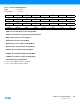
Table 29-2. I/O Lines Description
Pin Name Pin Description Type
TWD Two-wire Serial Data Input/Output
TWCK Two-wire Serial Clock Input/Output