
Datasheet


102
SAM7X Series [DATASHEET]
6120K–ATARM–11-Feb-14
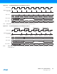
Figure 19-4. Code Read Optimization in Thumb Mode for FWS = 3
Note: When FWS is equal to 2 or 3, in case of sequential reads, the first access takes FWS cycles, the second access one
cycle, the third access FWS cycles, the fourth access one cycle, etc.
19.2.3 Write Operations
The internal memory area reserved for the embedded Flash can also be written through a write-only latch buffer. Write
operations take into account only the 8 lowest address bits and thus wrap around within the internal memory area
address space and appear to be repeated 1024 times within it.
Write operations can be prevented by programming the Memory Protection Unit of the product.
Writing 8-bit and 16-bit data is not allowed and may lead to unpredictable data corruption.
Write operations are performed in the number of wait states equal to the number of wait states for read operations + 1,
except for FWS = 3 (see “MC Flash Mode Register” on page 108).
19.2.4 Flash Commands
The EFC offers a command set to manage programming the memory flash, locking and unlocking lock sectors,
consecutive programming and locking, and full Flash erasing.
To run one of these commands, the field FCMD of the MC_FCR register has to be written with the command number. As
soon as the MC_FCR register is written, the FRDY flag is automatically cleared. Once the current command is achieved,
then the FRDY flag is automatically set. If an interrupt has been enabled by setting the bit FRDY in MC_FMR, the
interrupt line of the Memory Controller is activated.
Flash Access
Master Clock
Data To ARM
0-1
@Byte 0
@2
Bytes 0-3
Bytes 4-7
Bytes 8-11 Bytes 12-15
Bytes 0-3
2-3
6-7
@4
8-9
10-11
4-5
@8
@12
Bytes 4-7
3 Wait State Cycles
Buffer (32 bits)
ARM Request (16-bit)
Code Fetch
Bytes 8-11
3 Wait State Cycles
3 Wait State Cycles 3 Wait State Cycles
@6
@10
12-13
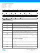
Table 19-2. Set of Commands
Command Value Mnemonic
Write page 0x01 WP
Set Lock Bit 0x02 SLB
Write Page and Lock 0x03 WPL
Clear Lock Bit 0x04 CLB
Erase all 0x08 EA
Set General-purpose NVM Bit 0x0B SGPB
Clear General-purpose NVM Bit 0x0D CGPB
Set Security Bit 0x0F SSB