AT91SAM7X-EK Evaluation Board for AT91SAM7X and AT91SAM7XC ..............................................................................................
6195E–ATARM–22-Mar-07 AT91SAM7X-EK Evaluation Board User Guide
Table of Contents Section 1 Overview............................................................................................... 1-1 1.1 1.2 1.3 Scope........................................................................................................1-1 Deliverables ..............................................................................................1-1 The AT91SAM7X-EK Evaluation Board....................................................
Section 6 Errata .................................................................................................... 6-1 6.1 Errata ........................................................................................................6-1 Section 7 Revision History.................................................................................... 7-1 7.1 ii 6195E–ATARM–22-Mar-07 Revision History ........................................................................................
Section 1 Overview 1.1 Scope The AT91SAM7X-EK and the AT91SAM7XC-EK evaluation kits enable evaluation capabilities and code development of applications running on the AT91SAM7X or the AT91SAM7XC microcontroller. This guide focuses on the AT91SAM7X-EK board as a common evaluation platform for the AT91SAM7X and AT91SAM7XC devices in a 100-lead LQFP package. 1.
Overview ! Power LED and general-purpose LEDs ! DataFlash® card slot ! expansion connector ! Atmel® serial DataFlash ! One footprint for Atmel Serial EEPROM (MN11) 1-2 6195E–ATARM–22-Mar-07 AT91SAM7X-EK Evaluation Board User Guide
Section 2 Setting Up the AT91SAM7X-EK Evaluation Board 2.1 Electrostatic Warning The AT91SAM7X-EK evaluation board is shipped in a protective anti-static package. The board must not be subjected to high electrostatic potentials. A grounding strap or similar protective device should be worn when handling the board. Avoid touching the component pins or any other metallic element. 2.
Setting Up the AT91SAM7X-EK Evaluation Board 2.3 Layout Figure 2-1.
Setting Up the AT91SAM7X-EK Evaluation Board Figure 2-2. Layout - Bottom View 2.4 Powering Up the Board The AT91SAM7X-EK board is self-powered by the USB port or by a USB power adapter. 2.5 Getting Started The AT91SAM7X-EK evaluation board is delivered with a DVD-ROM containing all necessary information and step-by-step procedures for working with the most common development tool chains. Please refer to this DVD-ROM, or to the AT91 web site, http://www.atmel.
Setting Up the AT91SAM7X-EK Evaluation Board 2.6 AT91SAM7X-EK Block Diagram Figure 2-3.
Section 3 Board Description 3.
Board Description – Power Optimization Capabilities, Including Slow Clock Mode (Down to 500 Hz) and Idle Mode – Four Programmable External Clock Signals ! Advanced Interrupt Controller (AIC) – Individually Maskable, Eight-level Priority, Vectored Interrupt Sources – Two External Interrupt Sources and One Fast Interrupt Source, Spurious Interrupt Protected ! Debug Unit (DBGU) – 2-wire UART and Support for Debug Communication Channel interrupt, Programmable ICE Access Prevention ! Periodic Interval Timer (PI
Board Description ! Two Universal Synchronous/Asynchronous Receiver Transmitters (USART) – Individual Baud Rate Generator, IrDA® Infrared Modulation/Demodulation – Support for ISO7816 T0/T1 Smart Card, Hardware Handshaking, RS485 Support – Full Modem Line Support on USART1 ! Two Master/Slave Serial Peripheral Interfaces (SPI) – 8- to 16-bit Programmable Data Length, Four External Peripheral Chip Selects ! One Three-channel 16-bit Timer/Counter (TC) – Three External Clock Inputs, Two Multi-purpose I/O Pins
Board Description 3.2 AT91SAM7X Block Diagram Figure 3-1. Block Diagram TDI TDO TMS TCK ICE JTAG SCAN ARM7TDMI Processor JTAGSEL 1.
Board Description 3.
Board Description – 12-bit key-protected Programmable Counter – Provides Reset or Interrupt Signals to the System – Counter May Be Stopped While the Processor is in Debug State or in Idle Mode ! Real-time Timer (RTT) – 32-bit Free-running Counter with Alarm – Runs Off the Internal RC Oscillator ! Two Parallel Input/Output Controllers (PIO) – Sixty-two Programmable I/O Lines Multiplexed with up to Two Peripheral I/Os – Input Change Interrupt Capability on Each I/O Line – Individually Programmable Open-drain
Board Description – 8- to 16-bit Programmable Data Length, Four External Peripheral Chip Selects ! One Three-channel 16-bit Timer/Counter (TC) – Three External Clock Inputs, Two Multi-purpose I/O Pins per Channel – Double PWM Generation, Capture/Waveform Mode, Up/Down Capability ! One Four-channel 16-bit Power Width Modulation Controller (PWMC) ! One Two-wire Interface (TWI) – Master Mode Support Only, All Two-wire Atmel EEPROMs Supported ! One 8-channel 10-bit Analog-to-Digital Converter, Four Channels Mu
Board Description 3.5 AT91SAM7XC Block Diagram Figure 3-2. Block Diagram TDI TDO TMS TCK ICE JTAG SCAN ARM7TDMI Processor JTAGSEL 1.
Board Description 3.6 Memory ! 256 Kbytes of Internal High-speed Flash ! 64 Kbytes of Internal High-speed SRAM ! Atmel serial DataFlash® ! One footprint for Atmel Serial EEPROM memory. The user can fit an AT24C128AN or AT24C256AN or AT24C512AN in 8S1 package as well as a cryptomemory AT88C25616C-SI 3.7 Clock Circuitry ! 18.432 MHz standard crystal for the embedded oscillator ! 32 KHz internal RC oscillator 3.
Board Description ! One yellow power LED (can also be software controlled) 3.13 Debug Interface ! 20-pin JTAG/ICE interface connector ! DBGU serial RS232 COM Port 3.14 Expansion Slot ! One DataFlash card slot ! All I/Os of the AT91SAM7X and the AT91SAM7XC are routed to peripheral extension connectors (J16). This allows the developer to check the integrity of the components and to extend the features of the board by adding external hardware components or boards.
Section 4 Configuration Straps 4.1 Configuration Straps Table 4-1. Configuration Jumpers and Straps Designation Default Setting J8 Opened Erases all internal Flash memory when the board is powered. To do that, the user will have to close the J8 at least 200 ms. J9 Opened Do not use: Factory test mode. J9 is not populated J10 Opened Selects ICE mode or JTAG mode (Closed). J10 is not populated.
Configuration Straps Table 4-1. Configuration Jumpers and Straps (Continued) Designation Default Setting S4 - S5 Closed Enables the use of 18.432MHz crystal. Must be open if an external clock is used. S6 Closed Enables the Power Led control (PB25). S7 Opened Disables Serial DataFlash write protect.
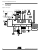
Section 5 Schematics 5.
8 7 6 5 4 3 2 3V3 1 JTAG INTERFACE MANUAL RESET USB DEVICE INTERFACE 3V3 8 7 6 5 S1 Closed by 0R resistor 3V3 J6 BP2 6 RR1 100K 1 J7 1 2 3 4 USB B 1 2 4 3 5 D 6 2 3V3 4 5 3V3 J10 J9 J8 3 1 3 5 7 9 11 13 15 17 19 3V3 DNP MN1 USBUF02W6 S2 3V3 2 4 6 8 10 12 14 16 18 20 D 3V3 NRST J11 3V3_ADC C2 100NF 10V 3 2 1 C1 10µF J13 J12 EN NR J15 5 4 15 37 62 87 3V3 3V3 C14 C15 C16 C17 C18 C19 C20 1µF 1µF 100NF 100NF 100NF 100NF 100NF C21 10NF TP1 S4 C22 10p
8 7 6 5 4 3 2 1 3V3 PA[0..
8 7 6 5 4 3 2 1 3V3 3V3 R21 D 10K Y2 1 OE D VDD 4 C45 100NF 50 MHz 2 VSS OUT 3 MII Factory setting SG-8002JC-50.0000M-PCB C46 22PF PB[0..
8 7 6 5 4 3 ATR2406 2.4 GHz RF CONNECTORS MODULE 2 1 USER'S GRID AERA Y4 SG-8002JC-13.8240M-PCB R35 10K 1 OE D 3V3 3V3 VDD 4 5V D 13.824 MHz 2 VSS 1.27 PITCH C61 100NF OUT 3 R36 0R RSSI R37 0R 3V3 PA[0..
Schematics 5-2 6195E–ATARM–22-Mar-07 AT91SAM7X-EK Evaluation Board User Guide
Section 6 Errata 6.1 DM9161A Ethernet Phy Connections The Ethernet interface works as presented in the schematics, but the connections are not in compliance with Davicom recommendations. To comply with Davicom recommendations on connecting this device, J27-4 and J27-5 (RJ45 connector, CT) should be connected to the VCCA side of L2. In the current schematics (ETHERNET, Sheet 3/4), the VCCA side of L2 is connected to MN10-1 and MN10-2 (DM9161A, AVDDR).
Errata 6-2 6195E–ATARM–22-Mar-07 AT91SAM7X-EK Evaluation Board User Guide
Section 7 Revision History 7.1 Revision History Table 7-1. Change History Change Request Ref. Document Comments 6195A First issue. 6195B Updated Figure 2-3 with new signal names. Updated document to show new product functionalities. New board block diagram and schematics issued. 6195C Updated document to contain new product AT91SAM7XC. Added new section with Errata. 6195D Removed references to 32 Mbit serial DataFlash (AT45DB321C-CNC) in Section 1.3 and in Section 3.6.
Revision History 7-2 6195E–ATARM–22-Mar-07 AT91SAM7X-EK Evaluation Board User Guide
Atmel Corporation 2325 Orchard Parkway San Jose, CA 95131, USA Tel: 1(408) 441-0311 Fax: 1(408) 487-2600 Regional Headquarters Atmel Europe Le Krebs 8, rue Jean-Pierre Timbaud BP 309 78054 Saint-Quentin-en-Yvelines Cedex France Tel: (33) 1-30-60-70-00 Fax: (33) 1-30-60-71-11 Asia Room 1219 Chinachem Golden Plaza 77 Mody Road Tsimshatsui East Kowloon Hong Kong Tel: (852) 2721-9778 Fax: (852) 2722-1369 Japan 9F, Tonetsu Shinkawa Bldg.