
Datasheet


Table Of Contents
- Features
- 1. Description
- 2. Block Diagram
- 3. Signal Description
- 4. Package and Pinout
- 5. Power Considerations
- 6. I/O Lines Considerations
- 7. Processor and Architecture
- 8. Memories
- 9. System Controller
- 10. Peripherals
- 10.1 User Interface
- 10.2 Peripheral Identifiers
- 10.3 Peripheral Multiplexing on PIO Lines
- 10.4 PIO Controller A Multiplexing
- 10.5 Serial Peripheral Interface
- 10.6 Two-wire Interface
- 10.7 USART
- 10.8 Serial Synchronous Controller
- 10.9 Timer Counter
- 10.10 PWM Controller
- 10.11 USB Device Port (Does not pertain to SAM7S32/16)
- 10.12 Analog-to-digital Converter
- 11. ARM7TDMI Processor Overview
- 12. Debug and Test Features
- 13. Reset Controller (RSTC)
- 14. Real-time Timer (RTT)
- 15. Periodic Interval Timer (PIT)
- 16. Watchdog Timer (WDT)
- 17. Voltage Regulator Mode Controller (VREG)
- 18. Memory Controller (MC)
- 19. Embedded Flash Controller (EFC)
- 20. Fast Flash Programming Interface (FFPI)
- 20.1 Overview
- 20.2 Parallel Fast Flash Programming
- 20.3 Serial Fast Flash Programming
- 21. SAM7 Boot Program
- 22. Peripheral DMA Controller (PDC)
- 22.1 Overview
- 22.2 Block Diagram
- 22.3 Functional Description
- 22.4 Peripheral DMA Controller (PDC) User Interface
- 22.4.1 PDC Receive Pointer Register
- 22.4.2 PDC Receive Counter Register
- 22.4.3 PDC Transmit Pointer Register
- 22.4.4 PDC Transmit Counter Register
- 22.4.5 PDC Receive Next Pointer Register
- 22.4.6 PDC Receive Next Counter Register
- 22.4.7 PDC Transmit Next Pointer Register
- 22.4.8 PDC Transmit Next Counter Register
- 22.4.9 PDC Transfer Control Register
- 22.4.10 PDC Transfer Status Register
- 23. Advanced Interrupt Controller (AIC)
- 23.1 Overview
- 23.2 Block Diagram
- 23.3 Application Block Diagram
- 23.4 AIC Detailed Block Diagram
- 23.5 I/O Line Description
- 23.6 Product Dependencies
- 23.7 Functional Description
- 23.8 Advanced Interrupt Controller (AIC) User Interface
- 23.8.1 Base Address
- 23.8.2 AIC Source Mode Register
- 23.8.3 AIC Source Vector Register
- 23.8.4 AIC Interrupt Vector Register
- 23.8.5 AIC FIQ Vector Register
- 23.8.6 AIC Interrupt Status Register
- 23.8.7 AIC Interrupt Pending Register
- 23.8.8 AIC Interrupt Mask Register
- 23.8.9 AIC Core Interrupt Status Register
- 23.8.10 AIC Interrupt Enable Command Register
- 23.8.11 AIC Interrupt Disable Command Register
- 23.8.12 AIC Interrupt Clear Command Register
- 23.8.13 AIC Interrupt Set Command Register
- 23.8.14 AIC End of Interrupt Command Register
- 23.8.15 AIC Spurious Interrupt Vector Register
- 23.8.16 AIC Debug Control Register
- 23.8.17 AIC Fast Forcing Enable Register
- 23.8.18 AIC Fast Forcing Disable Register
- 23.8.19 AIC Fast Forcing Status Register
- 24. Clock Generator
- 25. Power Management Controller (PMC)
- 25.1 Description
- 25.2 Master Clock Controller
- 25.3 Processor Clock Controller
- 25.4 USB Clock Controller
- 25.5 Peripheral Clock Controller
- 25.6 Programmable Clock Output Controller
- 25.7 Programming Sequence
- 25.8 Clock Switching Details
- 25.9 Power Management Controller (PMC) User Interface
- 25.9.1 PMC System Clock Enable Register
- 25.9.2 PMC System Clock Disable Register
- 25.9.3 PMC System Clock Status Register
- 25.9.4 PMC Peripheral Clock Enable Register
- 25.9.5 PMC Peripheral Clock Disable Register
- 25.9.6 PMC Peripheral Clock Status Register
- 25.9.7 PMC Clock Generator Main Oscillator Register
- 25.9.8 PMC Clock Generator Main Clock Frequency Register
- 25.9.9 PMC Clock Generator PLL Register
- 25.9.10 PMC Master Clock Register
- 25.9.11 PMC Programmable Clock Register
- 25.9.12 PMC Interrupt Enable Register
- 25.9.13 PMC Interrupt Disable Register
- 25.9.14 PMC Status Register
- 25.9.15 PMC Interrupt Mask Register
- 26. Debug Unit (DBGU)
- 26.1 Overview
- 26.2 Block Diagram
- 26.3 Product Dependencies
- 26.4 UART Operations
- 26.5 Debug Unit (DBGU) User Interface
- 26.5.1 Debug Unit Control Register
- 26.5.2 Debug Unit Mode Register
- 26.5.3 Debug Unit Interrupt Enable Register
- 26.5.4 Debug Unit Interrupt Disable Register
- 26.5.5 Debug Unit Interrupt Mask Register
- 26.5.6 Debug Unit Status Register
- 26.5.7 Debug Unit Receiver Holding Register
- 26.5.8 Debug Unit Transmit Holding Register
- 26.5.9 Debug Unit Baud Rate Generator Register
- 26.5.10 Debug Unit Chip ID Register
- 26.5.11 Debug Unit Chip ID Extension Register
- 26.5.12 Debug Unit Force NTRST Register
- 27. Parallel Input/Output Controller (PIO)
- 27.1 Overview
- 27.2 Block Diagram
- 27.3 Product Dependencies
- 27.4 Functional Description
- 27.4.1 Pull-up Resistor Control
- 27.4.2 I/O Line or Peripheral Function Selection
- 27.4.3 Peripheral A or B Selection
- 27.4.4 Output Control
- 27.4.5 Synchronous Data Output
- 27.4.6 Multi Drive Control (Open Drain)
- 27.4.7 Output Line Timings
- 27.4.8 Inputs
- 27.4.9 Input Glitch Filtering
- 27.4.10 Input Change Interrupt
- 27.5 I/O Lines Programming Example
- 27.6 Programmable Multibit ECC Error Location (PIO) User Interface
- 27.6.1 PIO Controller PIO Enable Register
- 27.6.2 PIO Controller PIO Disable Register
- 27.6.3 PIO Controller PIO Status Register
- 27.6.4 PIO Controller Output Enable Register
- 27.6.5 PIO Controller Output Disable Register
- 27.6.6 PIO Controller Output Status Register
- 27.6.7 PIO Controller Input Filter Enable Register
- 27.6.8 PIO Controller Input Filter Disable Register
- 27.6.9 PIO Controller Input Filter Status Register
- 27.6.10 PIO Controller Set Output Data Register
- 27.6.11 PIO Controller Clear Output Data Register
- 27.6.12 PIO Controller Output Data Status Register
- 27.6.13 PIO Controller Pin Data Status Register
- 27.6.14 PIO Controller Interrupt Enable Register
- 27.6.15 PIO Controller Interrupt Disable Register
- 27.6.16 PIO Controller Interrupt Mask Register
- 27.6.17 PIO Controller Interrupt Status Register
- 27.6.18 PIO Multi-driver Enable Register
- 27.6.19 PIO Multi-driver Disable Register
- 27.6.20 PIO Multi-driver Status Register
- 27.6.21 PIO Pull Up Disable Register
- 27.6.22 PIO Pull Up Enable Register
- 27.6.23 PIO Pull Up Status Register
- 27.6.24 PIO Peripheral A Select Register
- 27.6.25 PIO Peripheral B Select Register
- 27.6.26 PIO Peripheral A B Status Register
- 27.6.27 PIO Output Write Enable Register
- 27.6.28 PIO Output Write Disable Register
- 27.6.29 PIO Output Write Status Register
- 28. Serial Peripheral Interface (SPI)
- 29. Two-wire Interface (TWI) SAM7S512/256/128/64/321/32
- 29.1 Overview
- 29.2 List of Abbreviations
- 29.3 Block Diagram
- 29.4 Application Block Diagram
- 29.5 Product Dependencies
- 29.6 Functional Description
- 29.7 Two-wire Interface (TWI) User Interface
- 29.7.1 TWI Control Register
- 29.7.2 TWI Master Mode Register
- 29.7.3 TWI Internal Address Register
- 29.7.4 TWI Clock Waveform Generator Register
- 29.7.5 TWI Status Register
- 29.7.6 TWI Interrupt Enable Register
- 29.7.7 TWI Interrupt Disable Register
- 29.7.8 TWI Interrupt Mask Register
- 29.7.9 TWI Receive Holding Register
- 29.7.10 TWI Transmit Holding Register
- 30. Two Wire Interface (TWI) SAM7S161/16
- 30.1 Overview
- 30.2 List of Abbreviations
- 30.3 Block Diagram
- 30.4 Application Block Diagram
- 30.5 Product Dependencies
- 30.6 Functional Description
- 30.7 Master Mode
- 30.8 Multi-master Mode
- 30.9 Slave Mode
- 30.10 Two-wire Interface (TWI) User Interface
- 30.10.1 TWI Control Register
- 30.10.2 TWI Master Mode Register
- 30.10.3 TWI Slave Mode Register
- 30.10.4 TWI Internal Address Register
- 30.10.5 TWI Clock Waveform Generator Register
- 30.10.6 TWI Status Register
- 30.10.7 TWI Interrupt Enable Register
- 30.10.8 TWI Interrupt Disable Register
- 30.10.9 TWI Interrupt Mask Register
- 30.10.10 TWI Receive Holding Register
- 30.10.11 TWI Transmit Holding Register
- 31. Universal Synchronous Asynchronous Receiver Transceiver (USART)
- 31.1 Overview
- 31.2 Block Diagram
- 31.3 Application Block Diagram
- 31.4 I/O Lines Description
- 31.5 Product Dependencies
- 31.6 Functional Description
- 31.6.1 Baud Rate Generator
- 31.6.2 Receiver and Transmitter Control
- 31.6.3 Synchronous and Asynchronous Modes
- 31.6.3.1 Transmitter Operations
- 31.6.3.2 Asynchronous Receiver
- 31.6.3.3 Synchronous Receiver
- 31.6.3.4 Receiver Operations
- 31.6.3.5 Parity
- 31.6.3.6 Multidrop Mode
- 31.6.3.7 Transmitter Timeguard
- 31.6.3.8 Receiver Time-out
- 31.6.3.9 Framing Error
- 31.6.3.10 Transmit Break
- 31.6.3.11 Receive Break
- 31.6.3.12 Hardware Handshaking
- 31.6.4 ISO7816 Mode
- 31.6.5 IrDA Mode
- 31.6.6 RS485 Mode
- 31.6.7 SAM7S512/256/128/64/321/161 Modem Mode
- 31.6.8 Test Modes
- 31.7 Universal Synchronous Asynchronous Receiver Transmitter (USART) User Interface
- 31.7.1 USART Control Register
- 31.7.2 USART Mode Register
- 31.7.3 USART Interrupt Enable Register
- 31.7.4 USART Interrupt Disable Register
- 31.7.5 USART Interrupt Mask Register
- 31.7.6 USART Channel Status Register
- 31.7.7 USART Receive Holding Register
- 31.7.8 USART Transmit Holding Register
- 31.7.9 USART Baud Rate Generator Register
- 31.7.10 USART Receiver Time-out Register
- 31.7.11 USART Transmitter Timeguard Register
- 31.7.12 USART FI DI RATIO Register
- 31.7.13 USART Number of Errors Register
- 31.7.14 USART IrDA FILTER Register
- 32. Synchronous Serial Controller (SSC)
- 32.1 Description
- 32.2 Block Diagram
- 32.3 Application Block Diagram
- 32.4 Pin Name List
- 32.5 Product Dependencies
- 32.6 Functional Description
- 32.7 SSC Application Examples
- 32.8 Syncrhronous Serial Controller (SSC) User Interface
- 32.8.1 SSC Control Register
- 32.8.2 SSC Clock Mode Register
- 32.8.3 SSC Receive Clock Mode Register
- 32.8.4 SSC Receive Frame Mode Register
- 32.8.5 SSC Transmit Clock Mode Register
- 32.8.6 SSC Transmit Frame Mode Register
- 32.8.7 SSC Receive Holding Register
- 32.8.8 SSC Transmit Holding Register
- 32.8.9 SSC Receive Synchronization Holding Register
- 32.8.10 SSC Transmit Synchronization Holding Register
- 32.8.11 SSC Receive Compare 0 Register
- 32.8.12 SSC Receive Compare 1 Register
- 32.8.13 SSC Status Register
- 32.8.14 SSC Interrupt Enable Register
- 32.8.15 SSC Interrupt Disable Register
- 32.8.16 SSC Interrupt Mask Register
- 33. Timer Counter (TC)
- 33.1 Overview
- 33.2 Block Diagram
- 33.3 Pin Name List
- 33.4 Product Dependencies
- 33.5 Functional Description
- 33.5.1 TC Description
- 33.5.2 16-bit Counter
- 33.5.3 Clock Selection
- 33.5.4 Clock Control
- 33.5.5 TC Operating Modes
- 33.5.6 Trigger
- 33.5.7 Capture Operating Mode
- 33.5.8 Capture Registers A and B
- 33.5.9 Trigger Conditions
- 33.5.10 Waveform Operating Mode
- 33.5.11 Waveform Selection
- 33.5.12 External Event/Trigger Conditions
- 33.5.13 Output Controller
- 33.6 Timer Counter (TC) User Interface
- 33.6.1 TC Block Control Register
- 33.6.2 TC Block Mode Register
- 33.6.3 TC Channel Control Register
- 33.6.4 TC Channel Mode Register: Capture Mode
- 33.6.5 TC Channel Mode Register: Waveform Mode
- 33.6.6 TC Counter Value Register
- 33.6.7 TC Register A
- 33.6.8 TC Register B
- 33.6.9 TC Register C
- 33.6.10 TC Status Register
- 33.6.11 TC Interrupt Enable Register
- 33.6.12 TC Interrupt Disable Register
- 33.6.13 TC Interrupt Mask Register
- 34. Pulse Width Modulation Controller (PWM)
- 34.1 overview
- 34.2 Block Diagram
- 34.3 I/O Lines Description
- 34.4 Product Dependencies
- 34.5 Functional Description
- 34.6 Pulse Width Modulation Controller (PWM) User Interface
- 34.6.1 PWM Mode Register
- 34.6.2 PWM Enable Register
- 34.6.3 PWM Disable Register
- 34.6.4 PWM Status Register
- 34.6.5 PWM Interrupt Enable Register
- 34.6.6 PWM Interrupt Disable Register
- 34.6.7 PWM Interrupt Mask Register
- 34.6.8 PWM Interrupt Status Register
- 34.6.9 PWM Channel Mode Register
- 34.6.10 PWM Channel Duty Cycle Register
- 34.6.11 PWM Channel Period Register
- 34.6.12 PWM Channel Counter Register
- 34.6.13 PWM Channel Update Register
- 35. USB Device Port (UDP)
- 35.1 Overview
- 35.2 Block Diagram
- 35.3 Product Dependencies
- 35.4 Typical Connection
- 35.5 Functional Description
- 35.5.1 USB V2.0 Full-speed Introduction
- 35.5.2 Handling Transactions with USB V2.0 Device Peripheral
- 35.5.2.1 Setup Transaction
- 35.5.2.2 Data IN Transaction
- 35.5.2.3 Using Endpoints Without Ping-pong Attributes
- 35.5.2.4 Using Endpoints With Ping-pong Attribute
- 35.5.2.5 Data OUT Transaction
- 35.5.2.6 Data OUT Transaction Without Ping-pong Attributes
- 35.5.2.7 Using Endpoints With Ping-pong Attributes
- 35.5.2.8 Stall Handshake
- 35.5.3 Controlling Device States
- 35.6 USB Device Port (UDP) User Interface
- 35.6.1 UDP Frame Number Register
- 35.6.2 UDP Global State Register
- 35.6.3 UDP Function Address Register
- 35.6.4 UDP Interrupt Enable Register
- 35.6.5 UDP Interrupt Disable Register
- 35.6.6 UDP Interrupt Mask Register
- 35.6.7 UDP Interrupt Status Register
- 35.6.8 UDP Interrupt Clear Register
- 35.6.9 UDP Reset Endpoint Register
- 35.6.10 UDP Endpoint Control and Status Register
- 35.6.11 UDP FIFO Data Register
- 35.6.12 UDP Transceiver Control Register
- 36. Analog-to-Digital Converter (ADC)
- 36.1 Overview
- 36.2 Block Diagram
- 36.3 Signal Description
- 36.4 Product Dependencies
- 36.5 Functional Description
- 36.6 Analog-to-Digital Converter (ADC) User Interface
- 36.6.1 ADC Control Register
- 36.6.2 ADC Mode Register
- 36.6.3 ADC Channel Enable Register
- 36.6.4 ADC Channel Disable Register
- 36.6.5 ADC Channel Status Register
- 36.6.6 ADC Status Register
- 36.6.7 ADC Last Converted Data Register
- 36.6.8 ADC Interrupt Enable Register
- 36.6.9 ADC Interrupt Disable Register
- 36.6.10 ADC Interrupt Mask Register
- 36.6.11 ADC Channel Data Register
- 37. SAM7S Electrical Characteristics
- 38. Mechanical Characteristics
- 39. SAM7S Ordering Information
- 40. Errata
- 40.1 Marking
- 40.2 Errata Summary by Product and Revision or Manufacturing Number
- 40.3 Errata Organization by Product and Revision or Manufacturing Number
- 40.4 SAM7S512 Errata - Revision A Parts
- 40.4.1 Analog-to-Digital Converter (ADC)
- 40.4.1.1 ADC: DRDY Bit Cleared
- 40.4.1.2 ADC: DRDY not Cleared on Disable
- 40.4.1.3 ADC: DRDY Possibly Skipped due to CDR Read
- 40.4.1.4 ADC: Possible Skip on DRDY when Disabling a Channel
- 40.4.1.5 ADC: GOVRE Bit is not Updated
- 40.4.1.6 ADC: GOVRE Bit is not Set when Reading CDR
- 40.4.1.7 ADC: GOVRE Bit is not Set when Disabling a Channel
- 40.4.1.8 ADC: OVRE Flag Behavior
- 40.4.1.9 ADC: EOC Set although Channel Disabled
- 40.4.1.10 ADC: Spurious Clear of EOC Flag
- 40.4.1.11 ADC: Sleep Mode
- 40.4.2 Embedded Flash Controller (EFC)
- 40.4.3 Parallel Input/Output Controller (PIO)
- 40.4.4 Pulse Width Modulation Controller (PWM)
- 40.4.5 Real Time Timer (RTT)
- 40.4.6 Serial Peripheral Interface (SPI)
- 40.4.6.1 SPI: Software Reset Must be Written Twice
- 40.4.6.2 SPI: Bad tx_ready Behavior when CSAAT = 1 and SCBR = 1
- 40.4.6.3 SPI: LASTXFER (Last Transfer) Behavior
- 40.4.6.4 SPI: SPCK Behavior in Master Mode
- 40.4.6.5 SPI: Chip Select and Fixed Mode
- 40.4.6.6 SPI: Baudrate Set to 1
- 40.4.6.7 SPI: Disable In Slave Mode
- 40.4.6.8 SPI: Bad Serial Clock Generation on 2nd Chip Select
- 40.4.7 Synchronous Serial Controller (SSC)
- 40.4.8 Two-wire Interface (TWI)
- 40.4.9 Universal Synchronous Asynchronous Receiver Transmitter (USART)
- 40.4.1 Analog-to-Digital Converter (ADC)
- 40.5 SAM7S512 Errata - Revision B Parts
- 40.5.1 Analog-to-Digital Converter (ADC)
- 40.5.1.1 ADC: DRDY Bit Cleared
- 40.5.1.2 ADC: DRDY not Cleared on Disable
- 40.5.1.3 ADC: DRDY Possibly Skipped due to CDR Read
- 40.5.1.4 ADC: Possible Skip on DRDY when Disabling a Channel
- 40.5.1.5 ADC: GOVRE Bit is not Updated
- 40.5.1.6 ADC: GOVRE Bit is not Set when Reading CDR
- 40.5.1.7 ADC: GOVRE Bit is not Set when Disabling a Channel
- 40.5.1.8 ADC: OVRE Flag Behavior
- 40.5.1.9 ADC: EOC Set although Channel Disabled
- 40.5.1.10 ADC: Spurious Clear of EOC Flag
- 40.5.1.11 ADC: Sleep Mode
- 40.5.2 Embedded Flash Controller (EFC)
- 40.5.3 Parallel Input/Output Controller (PIO)
- 40.5.4 Pulse Width Modulation Controller (PWM)
- 40.5.5 Real Time Timer (RTT)
- 40.5.6 Serial Peripheral Interface (SPI)
- 40.5.6.1 SPI: Software Reset Must be Written Twice
- 40.5.6.2 SPI: Bad tx_ready Behavior when CSAAT = 1 and SCBR = 1
- 40.5.6.3 SPI: LASTXFER (Last Transfer) Behavior
- 40.5.6.4 SPI: SPCK Behavior in Master Mode
- 40.5.6.5 SPI: Chip Select and Fixed Mode
- 40.5.6.6 SPI: Baudrate Set to 1
- 40.5.6.7 SPI: Disable In Slave Mode
- 40.5.6.8 SPI: Bad Serial Clock Generation on 2nd Chip Select
- 40.5.7 Synchronous Serial Controller (SSC)
- 40.5.8 Two-wire Interface (TWI)
- 40.5.9 Universal Synchronous Asynchronous Receiver Transmitter (USART)
- 40.5.1 Analog-to-Digital Converter (ADC)
- 40.6 SAM7S256 Errata - Manufacturing Number 58818C
- 40.6.1 Chip ID
- 40.6.2 Analog-to-Digital Converter (ADC)
- 40.6.2.1 ADC: DRDY Bit Cleared
- 40.6.2.2 ADC: DRDY not Cleared on Disable
- 40.6.2.3 ADC: DRDY Possibly Skipped due to CDR Read
- 40.6.2.4 ADC: Possible Skip on DRDY when Disabling a Channel
- 40.6.2.5 ADC: GOVRE Bit is not Updated
- 40.6.2.6 ADC: GOVRE Bit is not Set when Reading CDR
- 40.6.2.7 ADC: GOVRE Bit is not Set when Disabling a Channel
- 40.6.2.8 ADC: OVRE Flag Behavior
- 40.6.2.9 ADC: EOC Set although Channel Disabled
- 40.6.2.10 ADC: Spurious Clear of EOC Flag
- 40.6.2.11 ADC: Sleep Mode
- 40.6.3 Master Clock (MCK)
- 40.6.4 Non Volatile Memory Bits (NVM Bits)
- 40.6.5 Parallel Input/Output Controller (PIO)
- 40.6.6 Power Management Controller (PMC)
- 40.6.7 Pulse Width Modulation Controller (PWM)
- 40.6.8 Real Time Timer (RTT)
- 40.6.9 Serial Peripheral Interface (SPI)
- 40.6.9.1 SPI: Bad tx_ready Behavior when CSAAT = 1 and SCBR = 1
- 40.6.9.2 SPI: LASTXFER (Last Transfer) Behavior
- 40.6.9.3 SPI: SPCK Behavior in Master Mode
- 40.6.9.4 SPI: Chip Select and Fixed Mode
- 40.6.9.5 SPI: Baudrate Set to 1
- 40.6.9.6 SPI: Disable In Slave Mode
- 40.6.9.7 SPI: Bad Serial Clock Generation on 2nd Chip Select
- 40.6.10 Synchronous Serial Controller (SSC)
- 40.6.11 Two-wire Interface (TWI)
- 40.6.12 Universal Synchronous Asynchronous Receiver Transmitter (USART)
- 40.6.13 Voltage Regulator
- 40.6.14 Watchdog Timer (WDT)
- 40.7 SAM7S256 Errata - Revision A Parts
- 40.7.1 Chip ID
- 40.7.2 Analog-to-Digital Converter (ADC)
- 40.7.2.1 ADC: DRDY Bit Cleared
- 40.7.2.2 ADC: DRDY not Cleared on Disable
- 40.7.2.3 ADC: DRDY Possibly Skipped due to CDR Read
- 40.7.2.4 ADC: Possible Skip on DRDY when Disabling a Channel
- 40.7.2.5 ADC: GOVRE Bit is not Updated
- 40.7.2.6 ADC: GOVRE Bit is not Set when Reading CDR
- 40.7.2.7 ADC: GOVRE Bit is not Set when Disabling a Channel
- 40.7.2.8 ADC: OVRE Flag Behavior
- 40.7.2.9 ADC: EOC Set although Channel Disabled
- 40.7.2.10 ADC: Spurious Clear of EOC Flag
- 40.7.2.11 ADC: Sleep Mode
- 40.7.3 Non Volatile Memory Bits (NVM Bits)
- 40.7.4 Parallel Input/Output Controller (PIO)
- 40.7.5 Power Management Controller (PMC)
- 40.7.6 Pulse Width Modulation Controller (PWM)
- 40.7.7 Real Time Timer (RTT)
- 40.7.8 Serial Peripheral Interface (SPI)
- 40.7.8.1 SPI: Bad tx_ready Behavior when CSAAT = 1 and SCBR = 1
- 40.7.8.2 SPI: LASTXFER (Last Transfer) Behavior
- 40.7.8.3 SPI: SPCK Behavior in Master Mode
- 40.7.8.4 SPI: Chip Select and Fixed Mode
- 40.7.8.5 SPI: Baudrate Set to 1
- 40.7.8.6 SPI: Disable In Slave Mode
- 40.7.8.7 SPI: Bad Serial Clock Generation on 2nd Chip Select
- 40.7.9 Synchronous Serial Controller (SSC)
- 40.7.10 Two-wire Interface (TWI)
- 40.7.11 Universal Synchronous Asynchronous Receiver Transmitter (USART)
- 40.7.12 Voltage Regulator
- 40.7.13 Watchdog Timer (WDT)
- 40.8 SAM7S256 Errata - Revision B Parts
- 40.8.1 Analog-to-Digital Converter (ADC)
- 40.8.1.1 ADC: DRDY Bit Cleared
- 40.8.1.2 ADC: DRDY not Cleared on Disable
- 40.8.1.3 ADC: DRDY Possibly Skipped due to CDR Read
- 40.8.1.4 ADC: Possible Skip on DRDY when Disabling a Channel
- 40.8.1.5 ADC: GOVRE Bit is not Updated
- 40.8.1.6 ADC: GOVRE Bit is not Set when Reading CDR
- 40.8.1.7 ADC: GOVRE Bit is not Set when Disabling a Channel
- 40.8.1.8 ADC: OVRE Flag Behavior
- 40.8.1.9 ADC: EOC Set although Channel Disabled
- 40.8.1.10 ADC: Spurious Clear of EOC Flag
- 40.8.1.11 ADC: Sleep Mode
- 40.8.2 Non Volatile Memory Bits (NVM Bits)
- 40.8.3 Parallel Input/Output Controller (PIO)
- 40.8.4 Pulse Width Modulation Controller (PWM)
- 40.8.5 Real Time Timer (RTT)
- 40.8.6 Serial Peripheral Interface (SPI)
- 40.8.6.1 SPI: Software Reset Must be Written Twice
- 40.8.6.2 SPI: Bad tx_ready Behavior when CSAAT = 1 and SCBR = 1
- 40.8.6.3 SPI: LASTXFER (Last Transfer) Behavior
- 40.8.6.4 SPI: SPCK Behavior in Master Mode
- 40.8.6.5 SPI: Chip Select and Fixed Mode
- 40.8.6.6 SPI: Baudrate Set to 1
- 40.8.6.7 SPI: Disable In Slave Mode
- 40.8.6.8 SPI: Bad Serial Clock Generation on 2nd Chip Select
- 40.8.7 Synchronous Serial Controller (SSC)
- 40.8.8 Two-wire Interface (TWI)
- 40.8.9 Universal Synchronous Asynchronous Receiver Transmitter (USART)
- 40.8.10 Voltage Regulator
- 40.8.1 Analog-to-Digital Converter (ADC)
- 40.9 SAM7S256 Errata - Revision C Parts
- 40.10 SAM7S256 Errata - Revision D Parts
- 40.11 SAM7S128 Errata - Manufacturing Number 58818C
- 40.11.1 Chip ID
- 40.11.2 Analog-to-Digital Converter (ADC)
- 40.11.2.1 ADC: DRDY Bit Cleared
- 40.11.2.2 ADC: DRDY not Cleared on Disable
- 40.11.2.3 ADC: DRDY Possibly Skipped due to CDR Read
- 40.11.2.4 ADC: Possible Skip on DRDY when Disabling a Channel
- 40.11.2.5 ADC: GOVRE Bit is not Updated
- 40.11.2.6 ADC: GOVRE Bit is not Set when Reading CDR
- 40.11.2.7 ADC: GOVRE Bit is not Set when Disabling a Channel
- 40.11.2.8 ADC: OVRE Flag Behavior
- 40.11.2.9 ADC: EOC Set although Channel Disabled
- 40.11.2.10 ADC: Spurious Clear of EOC Flag
- 40.11.2.11 ADC: Sleep Mode
- 40.11.3 Master Clock (MCK)
- 40.11.4 Non Volatile Memory Bits (NVM Bits)
- 40.11.5 Parallel Input/Output Controller (PIO)
- 40.11.6 Power Management Controller (PMC)
- 40.11.7 Pulse Width Modulation Controller (PWM)
- 40.11.8 Real Time Timer (RTT)
- 40.11.9 Serial Peripheral Interface (SPI)
- 40.11.9.1 SPI: Bad tx_ready behavior when CSAAT = 1 and SCBR = 1
- 40.11.9.2 SPI: LASTXFER (Last Transfer) behavior
- 40.11.9.3 SPI: SPCK Behavior in Master Mode
- 40.11.9.4 SPI: Chip Select and Fixed Mode
- 40.11.9.5 SPI: Baudrate Set to 1
- 40.11.9.6 SPI: Disable In Slave Mode
- 40.11.9.7 SPI: Bad Serial Clock Generation on 2nd Chip Select
- 40.11.10 Synchronous Serial Controller (SSC)
- 40.11.11 Two-wire Interface (TWI)
- 40.11.12 USART: Universal Synchronous Asynchronous Receiver Transmitter
- 40.11.13 Voltage Regulator
- 40.11.14 Watchdog Timer (WDT)
- 40.12 SAM7S128 Errata - Revision A Parts
- 40.12.1 Chip ID
- 40.12.2 Analog-to-Digital Converter (ADC)
- 40.12.2.1 ADC: DRDY Bit Cleared
- 40.12.2.2 ADC: DRDY not Cleared on Disable
- 40.12.2.3 ADC: DRDY Possibly Skipped due to CDR Read
- 40.12.2.4 ADC: Possible Skip on DRDY when Disabling a Channel
- 40.12.2.5 ADC: GOVRE Bit is not Updated
- 40.12.2.6 ADC: GOVRE Bit is not Set when Reading CDR
- 40.12.2.7 ADC: GOVRE Bit is not Set when Disabling a Channel
- 40.12.2.8 ADC: OVRE Flag Behavior
- 40.12.2.9 ADC: EOC Set although Channel Disabled
- 40.12.2.10 ADC: Spurious Clear of EOC Flag
- 40.12.2.11 ADC: Sleep Mode
- 40.12.3 Non Volatile Memory Bits (NVM Bits)
- 40.12.4 Parallel Input/Output Controller (PIO)
- 40.12.5 Power Management Controller (PMC)
- 40.12.6 Pulse Width Modulation Controller (PWM)
- 40.12.7 Real Time Timer (RTT)
- 40.12.8 Serial Peripheral Interface (SPI)
- 40.12.8.1 SPI: Bad tx_ready behavior when CSAAT = 1 and SCBR = 1
- 40.12.8.2 SPI: LASTXFER (Last Transfer) behavior
- 40.12.8.3 SPI: SPCK Behavior in Master Mode
- 40.12.8.4 SPI: Chip Select and Fixed Mode
- 40.12.8.5 SPI: Baudrate Set to 1
- 40.12.8.6 SPI: Disable In Slave Mode
- 40.12.8.7 SPI: Bad Serial Clock Generation on 2nd Chip Select
- 40.12.9 Synchronous Serial Controller (SSC)
- 40.12.10 Two-wire Interface (TWI)
- 40.12.11 USART: Universal Synchronous Asynchronous Receiver Transmitter
- 40.12.12 Voltage Regulator
- 40.12.13 Watchdog Timer (WDT)
- 40.13 SAM7S128 Errata - Revision B Parts
- 40.13.1 Analog-to-Digital Converter (ADC)
- 40.13.1.1 ADC: DRDY Bit Cleared
- 40.13.1.2 ADC: DRDY not Cleared on Disable
- 40.13.1.3 ADC: DRDY Possibly Skipped due to CDR Read
- 40.13.1.4 ADC: Possible Skip on DRDY when Disabling a Channel
- 40.13.1.5 ADC: GOVRE Bit is not Updated
- 40.13.1.6 ADC: GOVRE Bit is not Set when Reading CDR
- 40.13.1.7 ADC: GOVRE Bit is not Set when Disabling a Channel
- 40.13.1.8 ADC: OVRE Flag Behavior
- 40.13.1.9 ADC: EOC Set although Channel Disabled
- 40.13.1.10 ADC: Spurious Clear of EOC Flag
- 40.13.1.11 ADC: Sleep Mode
- 40.13.2 Non Volatile Memory Bits (NVM Bits)
- 40.13.3 Parallel Input/Output Controller (PIO)
- 40.13.4 Pulse Width Modulation Controller (PWM)
- 40.13.5 Real Time Timer (RTT)
- 40.13.6 Serial Peripheral Interface (SPI)
- 40.13.6.1 SPI: Software Reset Must be Written Twice
- 40.13.6.2 SPI: Bad tx_ready behavior when CSAAT = 1 and SCBR = 1
- 40.13.6.3 SPI: LASTXFER (Last Transfer) behavior
- 40.13.6.4 SPI: SPCK Behavior in Master Mode
- 40.13.6.5 SPI: Chip Select and Fixed Mode
- 40.13.6.6 SPI: Baudrate Set to 1
- 40.13.6.7 SPI: Disable In Slave Mode
- 40.13.6.8 SPI: Bad Serial Clock Generation on 2nd Chip Select
- 40.13.7 Synchronous Serial Controller (SSC)
- 40.13.8 Two-wire Interface (TWI)
- 40.13.9 USART: Universal Synchronous Asynchronous Receiver Transmitter
- 40.13.10 Voltage Regulator
- 40.13.1 Analog-to-Digital Converter (ADC)
- 40.14 SAM7S128 Errata - Revision C Parts
- 40.15 SAM7S128 Errata - Revision D Parts
- 40.16 SAM7S64 Errata - Manufacturing Number 58814G
- 40.16.1 Analog-to-Digital Converter (ADC)
- 40.16.1.1 ADC: DRDY Bit Cleared
- 40.16.1.2 ADC: DRDY not Cleared on Disable
- 40.16.1.3 ADC: DRDY Possibly Skipped due to CDR Read
- 40.16.1.4 ADC: Possible Skip on DRDY when Disabling a Channel
- 40.16.1.5 ADC: GOVRE Bit is not Updated
- 40.16.1.6 ADC: GOVRE Bit is not Set when Reading CDR
- 40.16.1.7 ADC: GOVRE Bit is not Set when Disabling a Channel
- 40.16.1.8 ADC: OVRE Flag Behavior
- 40.16.1.9 ADC: EOC Set although Channel Disabled
- 40.16.1.10 ADC: Spurious Clear of EOC Flag
- 40.16.1.11 ADC: Sleep Mode
- 40.16.2 JTAG
- 40.16.3 Master Clock (MCK)
- 40.16.4 Non Volatile Memory Bits (NVM Bits)
- 40.16.5 Parallel Input/Output Controller (PIO)
- 40.16.6 Pulse Width Modulation Controller (PWM)
- 40.16.7 Real Time Timer (RTT)
- 40.16.8 Serial Peripheral Interface (SPI)
- 40.16.8.1 20. SPI: Pulse Generation on SPCK
- 40.16.8.2 SPI: Bad tx_ready behavior when CSAAT=1 and SCBR = 1
- 40.16.8.3 SPI: LASTXFER (Last Transfer) behavior
- 40.16.8.4 SPI: SPCK Behavior in Master Mode
- 40.16.8.5 SPI: Chip Select and Fixed Mode
- 40.16.8.6 SPI: Baudrate Set to 1
- 40.16.8.7 SPI: Disable In Slave Mode
- 40.16.8.8 SPI: Disable Issue
- 40.16.8.9 SPI: Software Reset and SPIEN Bit
- 40.16.8.10 SPI: CSAAT = 1 and Delay
- 40.16.8.11 SPI: Bad Serial Clock Generation on 2nd Chip Select
- 40.16.9 Synchronous Serial Controller (SSC)
- 40.16.10 Two-wire Interface (TWI)
- 40.16.11 Universal Synchronous Asynchronous Receiver Transmitter (USART)
- 40.16.12 Voltage Regulator
- 40.16.1 Analog-to-Digital Converter (ADC)
- 40.17 SAM7S64 Errata - Revision A Parts
- 40.17.1 Analog-to-Digital Converter (ADC)
- 40.17.1.1 ADC: DRDY Bit Cleared
- 40.17.1.2 ADC: DRDY not Cleared on Disable
- 40.17.1.3 ADC: DRDY Possibly Skipped due to CDR Read
- 40.17.1.4 ADC: Possible Skip on DRDY when Disabling a Channel
- 40.17.1.5 ADC: GOVRE Bit is not Updated
- 40.17.1.6 ADC: GOVRE Bit is not Set when Reading CDR
- 40.17.1.7 ADC: GOVRE Bit is not Set when Disabling a Channel
- 40.17.1.8 ADC: OVRE Flag Behavior
- 40.17.1.9 ADC: EOC Set although Channel Disabled
- 40.17.1.10 ADC: Spurious Clear of EOC Flag
- 40.17.1.11 ADC: Sleep Mode
- 40.17.2 Non Volatile Memory Bits (NVM Bits)
- 40.17.3 Parallel Input/Output Controller (PIO)
- 40.17.4 Pulse Width Modulation Controller (PWM)
- 40.17.5 Real Time Timer (RTT)
- 40.17.6 Serial Peripheral Interface (SPI)
- 40.17.6.1 20. SPI: Pulse Generation on SPCK
- 40.17.6.2 SPI: Bad tx_ready behavior when CSAAT=1 and SCBR = 1
- 40.17.6.3 SPI: LASTXFER (Last Transfer) behavior
- 40.17.6.4 SPI: SPCK Behavior in Master Mode
- 40.17.6.5 SPI: Chip Select and Fixed Mode
- 40.17.6.6 SPI: Baudrate Set to 1
- 40.17.6.7 SPI: Disable In Slave Mode
- 40.17.6.8 SPI: Disable Issue
- 40.17.6.9 SPI: Software Reset and SPIEN Bit
- 40.17.6.10 SPI: CSAAT = 1 and Delay
- 40.17.6.11 SPI: Bad Serial Clock Generation on 2nd Chip Select
- 40.17.7 Synchronous Serial Controller (SSC)
- 40.17.8 Two-wire Interface (TWI)
- 40.17.9 Universal Synchronous Asynchronous Receiver Transmitter (USART)
- 40.17.10 Voltage Regulator
- 40.17.1 Analog-to-Digital Converter (ADC)
- 40.18 SAM7S64 Errata - Revision B Parts
- 40.18.1 Analog-to-Digital Converter (ADC)
- 40.18.1.1 ADC: DRDY Bit Cleared
- 40.18.1.2 ADC: DRDY not Cleared on Disable
- 40.18.1.3 ADC: DRDY Possibly Skipped due to CDR Read
- 40.18.1.4 ADC: Possible Skip on DRDY when Disabling a Channel
- 40.18.1.5 ADC: GOVRE Bit is not Updated
- 40.18.1.6 ADC: GOVRE Bit is not Set when Reading CDR
- 40.18.1.7 ADC: GOVRE Bit is not Set when Disabling a Channel
- 40.18.1.8 ADC: OVRE Flag Behavior
- 40.18.1.9 ADC: EOC Set although Channel Disabled
- 40.18.1.10 ADC: Spurious Clear of EOC Flag
- 40.18.1.11 ADC: Sleep Mode
- 40.18.2 Non Volatile Memory Bits (NVM Bits)
- 40.18.3 Parallel Input/Output Controller (PIO)
- 40.18.4 Pulse Width Modulation Controller (PWM)
- 40.18.5 Real Time Timer (RTT)
- 40.18.6 Serial Peripheral Interface (SPI)
- 40.18.6.1 SPI: Software Reset Must be Written Twice
- 40.18.6.2 SPI: Pulse Generation on SPCK
- 40.18.6.3 SPI: Bad tx_ready behavior when CSAAT=1 and SCBR = 1
- 40.18.6.4 SPI: LASTXFER (Last Transfer) behavior
- 40.18.6.5 SPI: SPCK Behavior in Master Mode
- 40.18.6.6 SPI: Chip Select and Fixed Mode
- 40.18.6.7 SPI: Baudrate Set to 1
- 40.18.6.8 SPI: Disable In Slave Mode
- 40.18.6.9 SPI: Disable Issue
- 40.18.6.10 SPI: Software Reset and SPIEN Bit
- 40.18.6.11 SPI: CSAAT = 1 and Delay
- 40.18.6.12 SPI: Bad Serial Clock Generation on 2nd Chip Select
- 40.18.7 Synchronous Serial Controller (SSC)
- 40.18.8 Two-wire Interface (TWI)
- 40.18.9 Universal Synchronous Asynchronous Receiver Transmitter (USART)
- 40.18.10 Voltage Regulator
- 40.18.1 Analog-to-Digital Converter (ADC)
- 40.19 SAM7S64 Errata - Revision C Parts
- 40.20 SAM7S321 Errata - Revision A Parts
- 40.20.1 Analog-to-Digital Converter (ADC)
- 40.20.1.1 ADC: DRDY Bit Cleared
- 40.20.1.2 ADC: DRDY not Cleared on Disable
- 40.20.1.3 ADC: DRDY Possibly Skipped due to CDR Read
- 40.20.1.4 ADC: Possible Skip on DRDY when Disabling a Channel
- 40.20.1.5 ADC: GOVRE Bit is not Updated
- 40.20.1.6 ADC: GOVRE Bit is not Set when Reading CDR
- 40.20.1.7 ADC: GOVRE Bit is not Set when Disabling a Channel
- 40.20.1.8 ADC: OVRE Flag Behavior
- 40.20.1.9 ADC: EOC Set although Channel Disabled
- 40.20.1.10 ADC: Spurious Clear of EOC Flag
- 40.20.1.11 ADC: Sleep Mode
- 40.20.2 Parallel Input/Output Controller (PIO)
- 40.20.3 Pulse Width Modulation Controller (PWM)
- 40.20.4 Real Time Timer (RTT)
- 40.20.5 Serial Peripheral Interface (SPI)
- 40.20.5.1 SPI: Software Reset Must be Written Twice
- 40.20.5.2 SPI: Pulse Generation on SPCK
- 40.20.5.3 SPI: Bad tx_ready behavior when CSAAT=1 and SCBR = 1
- 40.20.5.4 SPI: LASTXFER (Last Transfer) behavior
- 40.20.5.5 SPI: SPCK Behavior in Master Mode
- 40.20.5.6 SPI: Chip Select and Fixed Mode
- 40.20.5.7 SPI: Baudrate Set to 1
- 40.20.5.8 SPI: Disable In Slave Mode
- 40.20.5.9 SPI: Bad Serial Clock Generation on 2nd Chip Select
- 40.20.6 Synchronous Serial Controller (SSC)
- 40.20.7 Two-wire Interface (TWI)
- 40.20.8 Universal Synchronous Asynchronous Receiver Transmitter (USART)
- 40.20.1 Analog-to-Digital Converter (ADC)
- 40.21 SAM7S32 Errata - Manufacturing Number 58814G
- 40.21.1 Analog-to-Digital Converter (ADC)
- 40.21.1.1 ADC: DRDY Bit Cleared
- 40.21.1.2 ADC: DRDY not Cleared on Disable
- 40.21.1.3 ADC: DRDY Possibly Skipped due to CDR Read
- 40.21.1.4 ADC: Possible Skip on DRDY when Disabling a Channel
- 40.21.1.5 ADC: GOVRE Bit is not Updated
- 40.21.1.6 ADC: GOVRE Bit is not Set when Reading CDR
- 40.21.1.7 ADC: GOVRE Bit is not Set when Disabling a Channel
- 40.21.1.8 ADC: OVRE Flag Behavior
- 40.21.1.9 ADC: EOC Set although Channel Disabled
- 40.21.1.10 ADC: Spurious Clear of EOC Flag
- 40.21.1.11 ADC: Sleep Mode
- 40.21.2 JTAG
- 40.21.3 Master Clock (MCK)
- 40.21.4 Non Volatile Memory Bits (NVM Bits)
- 40.21.5 Parallel Input/Output Controller (PIO)
- 40.21.6 Pulse Width Modulation Controller (PWM)
- 40.21.7 Serial Peripheral Interface (SPI)
- 40.21.7.1 SPI: Pulse Generation on SPCK
- 40.21.7.2 SPI: Bad tx_ready behavior when CSAAT=1 and SCBR = 1
- 40.21.7.3 SPI: LASTXFER (Last Transfer) behavior
- 40.21.7.4 SPI: SPCK Behavior in Master Mode
- 40.21.7.5 SPI: Chip Select and Fixed Mode
- 40.21.7.6 SPI: Baudrate Set to 1
- 40.21.7.7 SPI: Disable In Slave Mode
- 40.21.7.8 SPI: Disable Issue
- 40.21.7.9 SPI: Software Reset and SPIEN Bit
- 40.21.7.10 SPI: CSAAT = 1 and Delay
- 40.21.7.11 SPI: Bad Serial Clock Generation on 2nd Chip Select
- 40.21.8 Synchronous Serial Controller (SSC)
- 40.21.9 Two-wire Interface (TWI)
- 40.21.10 Universal Synchronous Asynchronous Receiver Transmitter (USART)
- 40.21.11 Voltage Regulator
- 40.21.1 Analog-to-Digital Converter (ADC)
- 40.22 SAM7S32 Errata - Revision A Parts
- 40.22.1 Analog-to-Digital Converter (ADC)
- 40.22.1.1 ADC: DRDY Bit Cleared
- 40.22.1.2 ADC: DRDY not Cleared on Disable
- 40.22.1.3 ADC: DRDY Possibly Skipped due to CDR Read
- 40.22.1.4 ADC: Possible Skip on DRDY when Disabling a Channel
- 40.22.1.5 ADC: GOVRE Bit is not Updated
- 40.22.1.6 ADC: GOVRE Bit is not Set when Reading CDR
- 40.22.1.7 ADC: GOVRE Bit is not Set when Disabling a Channel
- 40.22.1.8 ADC: OVRE Flag Behavior
- 40.22.1.9 ADC: EOC Set although Channel Disabled
- 40.22.1.10 ADC: Spurious Clear of EOC Flag
- 40.22.1.11 ADC: Sleep Mode
- 40.22.2 Non Volatile Memory Bits (NVM Bits)
- 40.22.3 Parallel Input/Output Controller (PIO)
- 40.22.4 Pulse Width Modulation Controller (PWM)
- 40.22.5 Real Time Timer (RTT)
- 40.22.6 Serial Peripheral Interface (SPI)
- 40.22.6.1 20. SPI: Pulse Generation on SPCK
- 40.22.6.2 SPI: Bad tx_ready behavior when CSAAT=1 and SCBR = 1
- 40.22.6.3 SPI: LASTXFER (Last Transfer) behavior
- 40.22.6.4 SPI: SPCK Behavior in Master Mode
- 40.22.6.5 SPI: Chip Select and Fixed Mode
- 40.22.6.6 SPI: Baudrate Set to 1
- 40.22.6.7 SPI: Disable In Slave Mode
- 40.22.6.8 SPI: Disable Issue
- 40.22.6.9 SPI: Software Reset and SPIEN Bit
- 40.22.6.10 SPI: CSAAT = 1 and Delay
- 40.22.6.11 SPI: Bad Serial Clock Generation on 2nd Chip Select
- 40.22.7 Synchronous Serial Controller (SSC)
- 40.22.8 Two-wire Interface (TWI)
- 40.22.9 Universal Synchronous Asynchronous Receiver Transmitter (USART)
- 40.22.10 Voltage Regulator
- 40.22.1 Analog-to-Digital Converter (ADC)
- 40.23 SAM7S32 Errata - Revision B Parts
- 40.23.1 Analog-to-Digital Converter (ADC)
- 40.23.1.1 ADC: DRDY Bit Cleared
- 40.23.1.2 ADC: DRDY not Cleared on Disable
- 40.23.1.3 ADC: DRDY Possibly Skipped due to CDR Read
- 40.23.1.4 ADC: Possible Skip on DRDY when Disabling a Channel
- 40.23.1.5 ADC: GOVRE Bit is not Updated
- 40.23.1.6 ADC: GOVRE Bit is not Set when Reading CDR
- 40.23.1.7 ADC: GOVRE Bit is not Set when Disabling a Channel
- 40.23.1.8 ADC: OVRE Flag Behavior
- 40.23.1.9 ADC: EOC Set although Channel Disabled
- 40.23.1.10 ADC: Spurious Clear of EOC Flag
- 40.23.1.11 ADC: Sleep Mode
- 40.23.2 Parallel Input/Output Controller (PIO)
- 40.23.3 Pulse Width Modulation Controller (PWM)
- 40.23.4 Real Time Timer (RTT)
- 40.23.5 Serial Peripheral Interface (SPI)
- 40.23.5.1 SPI: Software Reset Must be Written Twice
- 40.23.5.2 20. SPI: Pulse Generation on SPCK
- 40.23.5.3 SPI: Bad tx_ready behavior when CSAAT=1 and SCBR = 1
- 40.23.5.4 SPI: LASTXFER (Last Transfer) behavior
- 40.23.5.5 SPI: SPCK Behavior in Master Mode
- 40.23.5.6 SPI: Chip Select and Fixed Mode
- 40.23.5.7 SPI: Baudrate Set to 1
- 40.23.5.8 SPI: Disable In Slave Mode
- 40.23.5.9 SPI: Disable Issue
- 40.23.5.10 SPI: Software Reset and SPIEN Bit
- 40.23.5.11 SPI: CSAAT = 1 and Delay
- 40.23.5.12 SPI: Bad Serial Clock Generation on 2nd Chip Select
- 40.23.6 Synchronous Serial Controller (SSC)
- 40.23.7 Two-wire Interface (TWI)
- 40.23.8 Universal Synchronous Asynchronous Receiver Transmitter (USART)
- 40.23.1 Analog-to-Digital Converter (ADC)
- 40.24 SAM7S161 Errata - Revision A Parts
- 40.24.1 Analog-to-Digital Converter (ADC)
- 40.24.1.1 ADC: DRDY Bit Cleared
- 40.24.1.2 ADC: DRDY not Cleared on Disable
- 40.24.1.3 ADC: DRDY Possibly Skipped due to CDR Read
- 40.24.1.4 ADC: Possible Skip on DRDY when Disabling a Channel
- 40.24.1.5 ADC: GOVRE Bit is not Updated
- 40.24.1.6 ADC: GOVRE Bit is not Set when Reading CDR
- 40.24.1.7 ADC: GOVRE Bit is not Set when Disabling a Channel
- 40.24.1.8 ADC: OVRE Flag Behavior
- 40.24.1.9 ADC: EOC Set although Channel Disabled
- 40.24.1.10 ADC: Spurious Clear of EOC Flag
- 40.24.1.11 ADC: Sleep Mode
- 40.24.2 Pulse Width Modulation Controller (PWM)
- 40.24.3 Real Time Timer (RTT)
- 40.24.4 Serial Peripheral Interface (SPI)
- 40.24.5 Synchronous Serial Controller (SSC)
- 40.24.6 Universal Synchronous Asynchronous Receiver Transmitter (USART)
- 40.24.1 Analog-to-Digital Converter (ADC)
- 40.25 SAM7S16 Errata - Revision A Parts
- 40.25.1 Analog-to-Digital Converter (ADC)
- 40.25.1.1 ADC: DRDY Bit Cleared
- 40.25.1.2 ADC: DRDY not Cleared on Disable
- 40.25.1.3 ADC: DRDY Possibly Skipped due to CDR Read
- 40.25.1.4 ADC: Possible Skip on DRDY when Disabling a Channel
- 40.25.1.5 ADC: GOVRE Bit is not Updated
- 40.25.1.6 ADC: GOVRE Bit is not Set when Reading CDR
- 40.25.1.7 ADC: GOVRE Bit is not Set when Disabling a Channel
- 40.25.1.8 ADC: OVRE Flag Behavior
- 40.25.1.9 ADC: EOC Set although Channel Disabled
- 40.25.1.10 ADC: Spurious Clear of EOC Flag
- 40.25.1.11 ADC: Sleep Mode
- 40.25.2 Pulse Width Modulation Controller (PWM)
- 40.25.3 Real Time Timer (RTT)
- 40.25.4 Serial Peripheral Interface (SPI)
- 40.25.5 Synchronous Serial Controller (SSC)
- 40.25.6 Universal Synchronous Asynchronous Receiver Transmitter (USART)
- 40.25.1 Analog-to-Digital Converter (ADC)
- Revision History
- Table of Contents
539
SAM7S Series [DATASHEET]
6175M–ATARM–26-Oct-12
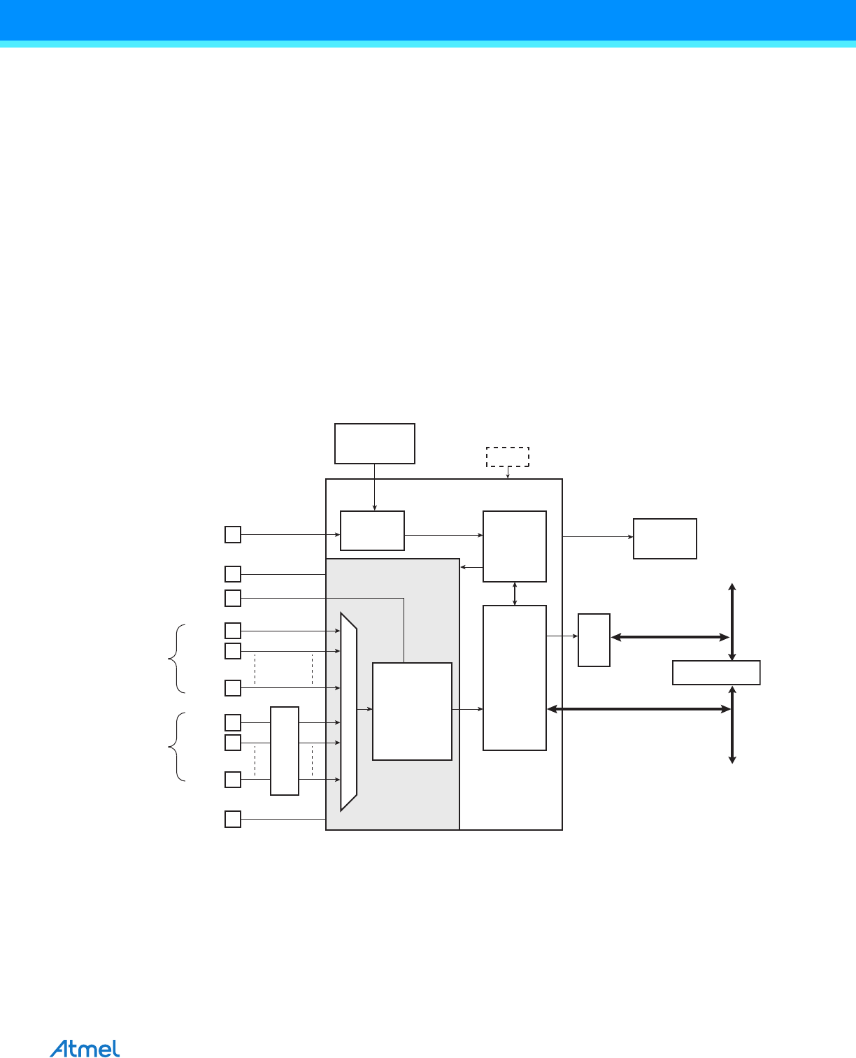
36. Analog-to-Digital Converter (ADC)
36.1 Overview
The ADC is based on a Successive Approximation Register (SAR) 10-bit Analog-to-Digital Converter (ADC). It also
integrates an 8-to-1 analog multiplexer, making possible the analog-to-digital conversions of 8 analog lines. The
conversions extend from 0V to ADVREF.
The ADC supports an 8-bit or 10-bit resolution mode, and conversion results are reported in a common register for
all channels, as well as in a channel-dedicated register. Software trigger, external trigger on rising edge of the
ADTRG pin or internal triggers from Timer Counter output(s) are configurable.
The ADC also integrates a Sleep Mode and a conversion sequencer and connects with a PDC channel. These fea-
tures reduce both power consumption and processor intervention.
Finally, the user can configure ADC timings, such as Startup Time and Sample & Hold Time.
36.2 Block Diagram
Figure 36-1. Analog-to-Digital Converter Block Diagram
ADC Interrupt
ADTRG
VDDIN
ADVREF
GND
Trigger
Selection
Control
Logic
Successive
Approximation
Register
Analog-to-Digital
Converter
Timer
Counter
Channels
User
Interface
AIC
Peripheral Bridge
APB
PDC
ASB
Dedicated
Analog
Inputs
Analog Inputs
Multiplexed
with I/O lines
AD-
AD-
AD-
PIO
AD-
AD-
AD-
ADC Controller
PMC
MCK
ADC cell