
Datasheet


Table Of Contents
- Features
- 1. Description
- 2. Block Diagram
- 3. Signal Description
- 4. Package and Pinout
- 5. Power Considerations
- 6. I/O Lines Considerations
- 7. Processor and Architecture
- 8. Memories
- 9. System Controller
- 10. Peripherals
- 10.1 User Interface
- 10.2 Peripheral Identifiers
- 10.3 Peripheral Multiplexing on PIO Lines
- 10.4 PIO Controller A Multiplexing
- 10.5 Serial Peripheral Interface
- 10.6 Two-wire Interface
- 10.7 USART
- 10.8 Serial Synchronous Controller
- 10.9 Timer Counter
- 10.10 PWM Controller
- 10.11 USB Device Port (Does not pertain to SAM7S32/16)
- 10.12 Analog-to-digital Converter
- 11. ARM7TDMI Processor Overview
- 12. Debug and Test Features
- 13. Reset Controller (RSTC)
- 14. Real-time Timer (RTT)
- 15. Periodic Interval Timer (PIT)
- 16. Watchdog Timer (WDT)
- 17. Voltage Regulator Mode Controller (VREG)
- 18. Memory Controller (MC)
- 19. Embedded Flash Controller (EFC)
- 20. Fast Flash Programming Interface (FFPI)
- 20.1 Overview
- 20.2 Parallel Fast Flash Programming
- 20.3 Serial Fast Flash Programming
- 21. SAM7 Boot Program
- 22. Peripheral DMA Controller (PDC)
- 22.1 Overview
- 22.2 Block Diagram
- 22.3 Functional Description
- 22.4 Peripheral DMA Controller (PDC) User Interface
- 22.4.1 PDC Receive Pointer Register
- 22.4.2 PDC Receive Counter Register
- 22.4.3 PDC Transmit Pointer Register
- 22.4.4 PDC Transmit Counter Register
- 22.4.5 PDC Receive Next Pointer Register
- 22.4.6 PDC Receive Next Counter Register
- 22.4.7 PDC Transmit Next Pointer Register
- 22.4.8 PDC Transmit Next Counter Register
- 22.4.9 PDC Transfer Control Register
- 22.4.10 PDC Transfer Status Register
- 23. Advanced Interrupt Controller (AIC)
- 23.1 Overview
- 23.2 Block Diagram
- 23.3 Application Block Diagram
- 23.4 AIC Detailed Block Diagram
- 23.5 I/O Line Description
- 23.6 Product Dependencies
- 23.7 Functional Description
- 23.8 Advanced Interrupt Controller (AIC) User Interface
- 23.8.1 Base Address
- 23.8.2 AIC Source Mode Register
- 23.8.3 AIC Source Vector Register
- 23.8.4 AIC Interrupt Vector Register
- 23.8.5 AIC FIQ Vector Register
- 23.8.6 AIC Interrupt Status Register
- 23.8.7 AIC Interrupt Pending Register
- 23.8.8 AIC Interrupt Mask Register
- 23.8.9 AIC Core Interrupt Status Register
- 23.8.10 AIC Interrupt Enable Command Register
- 23.8.11 AIC Interrupt Disable Command Register
- 23.8.12 AIC Interrupt Clear Command Register
- 23.8.13 AIC Interrupt Set Command Register
- 23.8.14 AIC End of Interrupt Command Register
- 23.8.15 AIC Spurious Interrupt Vector Register
- 23.8.16 AIC Debug Control Register
- 23.8.17 AIC Fast Forcing Enable Register
- 23.8.18 AIC Fast Forcing Disable Register
- 23.8.19 AIC Fast Forcing Status Register
- 24. Clock Generator
- 25. Power Management Controller (PMC)
- 25.1 Description
- 25.2 Master Clock Controller
- 25.3 Processor Clock Controller
- 25.4 USB Clock Controller
- 25.5 Peripheral Clock Controller
- 25.6 Programmable Clock Output Controller
- 25.7 Programming Sequence
- 25.8 Clock Switching Details
- 25.9 Power Management Controller (PMC) User Interface
- 25.9.1 PMC System Clock Enable Register
- 25.9.2 PMC System Clock Disable Register
- 25.9.3 PMC System Clock Status Register
- 25.9.4 PMC Peripheral Clock Enable Register
- 25.9.5 PMC Peripheral Clock Disable Register
- 25.9.6 PMC Peripheral Clock Status Register
- 25.9.7 PMC Clock Generator Main Oscillator Register
- 25.9.8 PMC Clock Generator Main Clock Frequency Register
- 25.9.9 PMC Clock Generator PLL Register
- 25.9.10 PMC Master Clock Register
- 25.9.11 PMC Programmable Clock Register
- 25.9.12 PMC Interrupt Enable Register
- 25.9.13 PMC Interrupt Disable Register
- 25.9.14 PMC Status Register
- 25.9.15 PMC Interrupt Mask Register
- 26. Debug Unit (DBGU)
- 26.1 Overview
- 26.2 Block Diagram
- 26.3 Product Dependencies
- 26.4 UART Operations
- 26.5 Debug Unit (DBGU) User Interface
- 26.5.1 Debug Unit Control Register
- 26.5.2 Debug Unit Mode Register
- 26.5.3 Debug Unit Interrupt Enable Register
- 26.5.4 Debug Unit Interrupt Disable Register
- 26.5.5 Debug Unit Interrupt Mask Register
- 26.5.6 Debug Unit Status Register
- 26.5.7 Debug Unit Receiver Holding Register
- 26.5.8 Debug Unit Transmit Holding Register
- 26.5.9 Debug Unit Baud Rate Generator Register
- 26.5.10 Debug Unit Chip ID Register
- 26.5.11 Debug Unit Chip ID Extension Register
- 26.5.12 Debug Unit Force NTRST Register
- 27. Parallel Input/Output Controller (PIO)
- 27.1 Overview
- 27.2 Block Diagram
- 27.3 Product Dependencies
- 27.4 Functional Description
- 27.4.1 Pull-up Resistor Control
- 27.4.2 I/O Line or Peripheral Function Selection
- 27.4.3 Peripheral A or B Selection
- 27.4.4 Output Control
- 27.4.5 Synchronous Data Output
- 27.4.6 Multi Drive Control (Open Drain)
- 27.4.7 Output Line Timings
- 27.4.8 Inputs
- 27.4.9 Input Glitch Filtering
- 27.4.10 Input Change Interrupt
- 27.5 I/O Lines Programming Example
- 27.6 Programmable Multibit ECC Error Location (PIO) User Interface
- 27.6.1 PIO Controller PIO Enable Register
- 27.6.2 PIO Controller PIO Disable Register
- 27.6.3 PIO Controller PIO Status Register
- 27.6.4 PIO Controller Output Enable Register
- 27.6.5 PIO Controller Output Disable Register
- 27.6.6 PIO Controller Output Status Register
- 27.6.7 PIO Controller Input Filter Enable Register
- 27.6.8 PIO Controller Input Filter Disable Register
- 27.6.9 PIO Controller Input Filter Status Register
- 27.6.10 PIO Controller Set Output Data Register
- 27.6.11 PIO Controller Clear Output Data Register
- 27.6.12 PIO Controller Output Data Status Register
- 27.6.13 PIO Controller Pin Data Status Register
- 27.6.14 PIO Controller Interrupt Enable Register
- 27.6.15 PIO Controller Interrupt Disable Register
- 27.6.16 PIO Controller Interrupt Mask Register
- 27.6.17 PIO Controller Interrupt Status Register
- 27.6.18 PIO Multi-driver Enable Register
- 27.6.19 PIO Multi-driver Disable Register
- 27.6.20 PIO Multi-driver Status Register
- 27.6.21 PIO Pull Up Disable Register
- 27.6.22 PIO Pull Up Enable Register
- 27.6.23 PIO Pull Up Status Register
- 27.6.24 PIO Peripheral A Select Register
- 27.6.25 PIO Peripheral B Select Register
- 27.6.26 PIO Peripheral A B Status Register
- 27.6.27 PIO Output Write Enable Register
- 27.6.28 PIO Output Write Disable Register
- 27.6.29 PIO Output Write Status Register
- 28. Serial Peripheral Interface (SPI)
- 29. Two-wire Interface (TWI) SAM7S512/256/128/64/321/32
- 29.1 Overview
- 29.2 List of Abbreviations
- 29.3 Block Diagram
- 29.4 Application Block Diagram
- 29.5 Product Dependencies
- 29.6 Functional Description
- 29.7 Two-wire Interface (TWI) User Interface
- 29.7.1 TWI Control Register
- 29.7.2 TWI Master Mode Register
- 29.7.3 TWI Internal Address Register
- 29.7.4 TWI Clock Waveform Generator Register
- 29.7.5 TWI Status Register
- 29.7.6 TWI Interrupt Enable Register
- 29.7.7 TWI Interrupt Disable Register
- 29.7.8 TWI Interrupt Mask Register
- 29.7.9 TWI Receive Holding Register
- 29.7.10 TWI Transmit Holding Register
- 30. Two Wire Interface (TWI) SAM7S161/16
- 30.1 Overview
- 30.2 List of Abbreviations
- 30.3 Block Diagram
- 30.4 Application Block Diagram
- 30.5 Product Dependencies
- 30.6 Functional Description
- 30.7 Master Mode
- 30.8 Multi-master Mode
- 30.9 Slave Mode
- 30.10 Two-wire Interface (TWI) User Interface
- 30.10.1 TWI Control Register
- 30.10.2 TWI Master Mode Register
- 30.10.3 TWI Slave Mode Register
- 30.10.4 TWI Internal Address Register
- 30.10.5 TWI Clock Waveform Generator Register
- 30.10.6 TWI Status Register
- 30.10.7 TWI Interrupt Enable Register
- 30.10.8 TWI Interrupt Disable Register
- 30.10.9 TWI Interrupt Mask Register
- 30.10.10 TWI Receive Holding Register
- 30.10.11 TWI Transmit Holding Register
- 31. Universal Synchronous Asynchronous Receiver Transceiver (USART)
- 31.1 Overview
- 31.2 Block Diagram
- 31.3 Application Block Diagram
- 31.4 I/O Lines Description
- 31.5 Product Dependencies
- 31.6 Functional Description
- 31.6.1 Baud Rate Generator
- 31.6.2 Receiver and Transmitter Control
- 31.6.3 Synchronous and Asynchronous Modes
- 31.6.3.1 Transmitter Operations
- 31.6.3.2 Asynchronous Receiver
- 31.6.3.3 Synchronous Receiver
- 31.6.3.4 Receiver Operations
- 31.6.3.5 Parity
- 31.6.3.6 Multidrop Mode
- 31.6.3.7 Transmitter Timeguard
- 31.6.3.8 Receiver Time-out
- 31.6.3.9 Framing Error
- 31.6.3.10 Transmit Break
- 31.6.3.11 Receive Break
- 31.6.3.12 Hardware Handshaking
- 31.6.4 ISO7816 Mode
- 31.6.5 IrDA Mode
- 31.6.6 RS485 Mode
- 31.6.7 SAM7S512/256/128/64/321/161 Modem Mode
- 31.6.8 Test Modes
- 31.7 Universal Synchronous Asynchronous Receiver Transmitter (USART) User Interface
- 31.7.1 USART Control Register
- 31.7.2 USART Mode Register
- 31.7.3 USART Interrupt Enable Register
- 31.7.4 USART Interrupt Disable Register
- 31.7.5 USART Interrupt Mask Register
- 31.7.6 USART Channel Status Register
- 31.7.7 USART Receive Holding Register
- 31.7.8 USART Transmit Holding Register
- 31.7.9 USART Baud Rate Generator Register
- 31.7.10 USART Receiver Time-out Register
- 31.7.11 USART Transmitter Timeguard Register
- 31.7.12 USART FI DI RATIO Register
- 31.7.13 USART Number of Errors Register
- 31.7.14 USART IrDA FILTER Register
- 32. Synchronous Serial Controller (SSC)
- 32.1 Description
- 32.2 Block Diagram
- 32.3 Application Block Diagram
- 32.4 Pin Name List
- 32.5 Product Dependencies
- 32.6 Functional Description
- 32.7 SSC Application Examples
- 32.8 Syncrhronous Serial Controller (SSC) User Interface
- 32.8.1 SSC Control Register
- 32.8.2 SSC Clock Mode Register
- 32.8.3 SSC Receive Clock Mode Register
- 32.8.4 SSC Receive Frame Mode Register
- 32.8.5 SSC Transmit Clock Mode Register
- 32.8.6 SSC Transmit Frame Mode Register
- 32.8.7 SSC Receive Holding Register
- 32.8.8 SSC Transmit Holding Register
- 32.8.9 SSC Receive Synchronization Holding Register
- 32.8.10 SSC Transmit Synchronization Holding Register
- 32.8.11 SSC Receive Compare 0 Register
- 32.8.12 SSC Receive Compare 1 Register
- 32.8.13 SSC Status Register
- 32.8.14 SSC Interrupt Enable Register
- 32.8.15 SSC Interrupt Disable Register
- 32.8.16 SSC Interrupt Mask Register
- 33. Timer Counter (TC)
- 33.1 Overview
- 33.2 Block Diagram
- 33.3 Pin Name List
- 33.4 Product Dependencies
- 33.5 Functional Description
- 33.5.1 TC Description
- 33.5.2 16-bit Counter
- 33.5.3 Clock Selection
- 33.5.4 Clock Control
- 33.5.5 TC Operating Modes
- 33.5.6 Trigger
- 33.5.7 Capture Operating Mode
- 33.5.8 Capture Registers A and B
- 33.5.9 Trigger Conditions
- 33.5.10 Waveform Operating Mode
- 33.5.11 Waveform Selection
- 33.5.12 External Event/Trigger Conditions
- 33.5.13 Output Controller
- 33.6 Timer Counter (TC) User Interface
- 33.6.1 TC Block Control Register
- 33.6.2 TC Block Mode Register
- 33.6.3 TC Channel Control Register
- 33.6.4 TC Channel Mode Register: Capture Mode
- 33.6.5 TC Channel Mode Register: Waveform Mode
- 33.6.6 TC Counter Value Register
- 33.6.7 TC Register A
- 33.6.8 TC Register B
- 33.6.9 TC Register C
- 33.6.10 TC Status Register
- 33.6.11 TC Interrupt Enable Register
- 33.6.12 TC Interrupt Disable Register
- 33.6.13 TC Interrupt Mask Register
- 34. Pulse Width Modulation Controller (PWM)
- 34.1 overview
- 34.2 Block Diagram
- 34.3 I/O Lines Description
- 34.4 Product Dependencies
- 34.5 Functional Description
- 34.6 Pulse Width Modulation Controller (PWM) User Interface
- 34.6.1 PWM Mode Register
- 34.6.2 PWM Enable Register
- 34.6.3 PWM Disable Register
- 34.6.4 PWM Status Register
- 34.6.5 PWM Interrupt Enable Register
- 34.6.6 PWM Interrupt Disable Register
- 34.6.7 PWM Interrupt Mask Register
- 34.6.8 PWM Interrupt Status Register
- 34.6.9 PWM Channel Mode Register
- 34.6.10 PWM Channel Duty Cycle Register
- 34.6.11 PWM Channel Period Register
- 34.6.12 PWM Channel Counter Register
- 34.6.13 PWM Channel Update Register
- 35. USB Device Port (UDP)
- 35.1 Overview
- 35.2 Block Diagram
- 35.3 Product Dependencies
- 35.4 Typical Connection
- 35.5 Functional Description
- 35.5.1 USB V2.0 Full-speed Introduction
- 35.5.2 Handling Transactions with USB V2.0 Device Peripheral
- 35.5.2.1 Setup Transaction
- 35.5.2.2 Data IN Transaction
- 35.5.2.3 Using Endpoints Without Ping-pong Attributes
- 35.5.2.4 Using Endpoints With Ping-pong Attribute
- 35.5.2.5 Data OUT Transaction
- 35.5.2.6 Data OUT Transaction Without Ping-pong Attributes
- 35.5.2.7 Using Endpoints With Ping-pong Attributes
- 35.5.2.8 Stall Handshake
- 35.5.3 Controlling Device States
- 35.6 USB Device Port (UDP) User Interface
- 35.6.1 UDP Frame Number Register
- 35.6.2 UDP Global State Register
- 35.6.3 UDP Function Address Register
- 35.6.4 UDP Interrupt Enable Register
- 35.6.5 UDP Interrupt Disable Register
- 35.6.6 UDP Interrupt Mask Register
- 35.6.7 UDP Interrupt Status Register
- 35.6.8 UDP Interrupt Clear Register
- 35.6.9 UDP Reset Endpoint Register
- 35.6.10 UDP Endpoint Control and Status Register
- 35.6.11 UDP FIFO Data Register
- 35.6.12 UDP Transceiver Control Register
- 36. Analog-to-Digital Converter (ADC)
- 36.1 Overview
- 36.2 Block Diagram
- 36.3 Signal Description
- 36.4 Product Dependencies
- 36.5 Functional Description
- 36.6 Analog-to-Digital Converter (ADC) User Interface
- 36.6.1 ADC Control Register
- 36.6.2 ADC Mode Register
- 36.6.3 ADC Channel Enable Register
- 36.6.4 ADC Channel Disable Register
- 36.6.5 ADC Channel Status Register
- 36.6.6 ADC Status Register
- 36.6.7 ADC Last Converted Data Register
- 36.6.8 ADC Interrupt Enable Register
- 36.6.9 ADC Interrupt Disable Register
- 36.6.10 ADC Interrupt Mask Register
- 36.6.11 ADC Channel Data Register
- 37. SAM7S Electrical Characteristics
- 38. Mechanical Characteristics
- 39. SAM7S Ordering Information
- 40. Errata
- 40.1 Marking
- 40.2 Errata Summary by Product and Revision or Manufacturing Number
- 40.3 Errata Organization by Product and Revision or Manufacturing Number
- 40.4 SAM7S512 Errata - Revision A Parts
- 40.4.1 Analog-to-Digital Converter (ADC)
- 40.4.1.1 ADC: DRDY Bit Cleared
- 40.4.1.2 ADC: DRDY not Cleared on Disable
- 40.4.1.3 ADC: DRDY Possibly Skipped due to CDR Read
- 40.4.1.4 ADC: Possible Skip on DRDY when Disabling a Channel
- 40.4.1.5 ADC: GOVRE Bit is not Updated
- 40.4.1.6 ADC: GOVRE Bit is not Set when Reading CDR
- 40.4.1.7 ADC: GOVRE Bit is not Set when Disabling a Channel
- 40.4.1.8 ADC: OVRE Flag Behavior
- 40.4.1.9 ADC: EOC Set although Channel Disabled
- 40.4.1.10 ADC: Spurious Clear of EOC Flag
- 40.4.1.11 ADC: Sleep Mode
- 40.4.2 Embedded Flash Controller (EFC)
- 40.4.3 Parallel Input/Output Controller (PIO)
- 40.4.4 Pulse Width Modulation Controller (PWM)
- 40.4.5 Real Time Timer (RTT)
- 40.4.6 Serial Peripheral Interface (SPI)
- 40.4.6.1 SPI: Software Reset Must be Written Twice
- 40.4.6.2 SPI: Bad tx_ready Behavior when CSAAT = 1 and SCBR = 1
- 40.4.6.3 SPI: LASTXFER (Last Transfer) Behavior
- 40.4.6.4 SPI: SPCK Behavior in Master Mode
- 40.4.6.5 SPI: Chip Select and Fixed Mode
- 40.4.6.6 SPI: Baudrate Set to 1
- 40.4.6.7 SPI: Disable In Slave Mode
- 40.4.6.8 SPI: Bad Serial Clock Generation on 2nd Chip Select
- 40.4.7 Synchronous Serial Controller (SSC)
- 40.4.8 Two-wire Interface (TWI)
- 40.4.9 Universal Synchronous Asynchronous Receiver Transmitter (USART)
- 40.4.1 Analog-to-Digital Converter (ADC)
- 40.5 SAM7S512 Errata - Revision B Parts
- 40.5.1 Analog-to-Digital Converter (ADC)
- 40.5.1.1 ADC: DRDY Bit Cleared
- 40.5.1.2 ADC: DRDY not Cleared on Disable
- 40.5.1.3 ADC: DRDY Possibly Skipped due to CDR Read
- 40.5.1.4 ADC: Possible Skip on DRDY when Disabling a Channel
- 40.5.1.5 ADC: GOVRE Bit is not Updated
- 40.5.1.6 ADC: GOVRE Bit is not Set when Reading CDR
- 40.5.1.7 ADC: GOVRE Bit is not Set when Disabling a Channel
- 40.5.1.8 ADC: OVRE Flag Behavior
- 40.5.1.9 ADC: EOC Set although Channel Disabled
- 40.5.1.10 ADC: Spurious Clear of EOC Flag
- 40.5.1.11 ADC: Sleep Mode
- 40.5.2 Embedded Flash Controller (EFC)
- 40.5.3 Parallel Input/Output Controller (PIO)
- 40.5.4 Pulse Width Modulation Controller (PWM)
- 40.5.5 Real Time Timer (RTT)
- 40.5.6 Serial Peripheral Interface (SPI)
- 40.5.6.1 SPI: Software Reset Must be Written Twice
- 40.5.6.2 SPI: Bad tx_ready Behavior when CSAAT = 1 and SCBR = 1
- 40.5.6.3 SPI: LASTXFER (Last Transfer) Behavior
- 40.5.6.4 SPI: SPCK Behavior in Master Mode
- 40.5.6.5 SPI: Chip Select and Fixed Mode
- 40.5.6.6 SPI: Baudrate Set to 1
- 40.5.6.7 SPI: Disable In Slave Mode
- 40.5.6.8 SPI: Bad Serial Clock Generation on 2nd Chip Select
- 40.5.7 Synchronous Serial Controller (SSC)
- 40.5.8 Two-wire Interface (TWI)
- 40.5.9 Universal Synchronous Asynchronous Receiver Transmitter (USART)
- 40.5.1 Analog-to-Digital Converter (ADC)
- 40.6 SAM7S256 Errata - Manufacturing Number 58818C
- 40.6.1 Chip ID
- 40.6.2 Analog-to-Digital Converter (ADC)
- 40.6.2.1 ADC: DRDY Bit Cleared
- 40.6.2.2 ADC: DRDY not Cleared on Disable
- 40.6.2.3 ADC: DRDY Possibly Skipped due to CDR Read
- 40.6.2.4 ADC: Possible Skip on DRDY when Disabling a Channel
- 40.6.2.5 ADC: GOVRE Bit is not Updated
- 40.6.2.6 ADC: GOVRE Bit is not Set when Reading CDR
- 40.6.2.7 ADC: GOVRE Bit is not Set when Disabling a Channel
- 40.6.2.8 ADC: OVRE Flag Behavior
- 40.6.2.9 ADC: EOC Set although Channel Disabled
- 40.6.2.10 ADC: Spurious Clear of EOC Flag
- 40.6.2.11 ADC: Sleep Mode
- 40.6.3 Master Clock (MCK)
- 40.6.4 Non Volatile Memory Bits (NVM Bits)
- 40.6.5 Parallel Input/Output Controller (PIO)
- 40.6.6 Power Management Controller (PMC)
- 40.6.7 Pulse Width Modulation Controller (PWM)
- 40.6.8 Real Time Timer (RTT)
- 40.6.9 Serial Peripheral Interface (SPI)
- 40.6.9.1 SPI: Bad tx_ready Behavior when CSAAT = 1 and SCBR = 1
- 40.6.9.2 SPI: LASTXFER (Last Transfer) Behavior
- 40.6.9.3 SPI: SPCK Behavior in Master Mode
- 40.6.9.4 SPI: Chip Select and Fixed Mode
- 40.6.9.5 SPI: Baudrate Set to 1
- 40.6.9.6 SPI: Disable In Slave Mode
- 40.6.9.7 SPI: Bad Serial Clock Generation on 2nd Chip Select
- 40.6.10 Synchronous Serial Controller (SSC)
- 40.6.11 Two-wire Interface (TWI)
- 40.6.12 Universal Synchronous Asynchronous Receiver Transmitter (USART)
- 40.6.13 Voltage Regulator
- 40.6.14 Watchdog Timer (WDT)
- 40.7 SAM7S256 Errata - Revision A Parts
- 40.7.1 Chip ID
- 40.7.2 Analog-to-Digital Converter (ADC)
- 40.7.2.1 ADC: DRDY Bit Cleared
- 40.7.2.2 ADC: DRDY not Cleared on Disable
- 40.7.2.3 ADC: DRDY Possibly Skipped due to CDR Read
- 40.7.2.4 ADC: Possible Skip on DRDY when Disabling a Channel
- 40.7.2.5 ADC: GOVRE Bit is not Updated
- 40.7.2.6 ADC: GOVRE Bit is not Set when Reading CDR
- 40.7.2.7 ADC: GOVRE Bit is not Set when Disabling a Channel
- 40.7.2.8 ADC: OVRE Flag Behavior
- 40.7.2.9 ADC: EOC Set although Channel Disabled
- 40.7.2.10 ADC: Spurious Clear of EOC Flag
- 40.7.2.11 ADC: Sleep Mode
- 40.7.3 Non Volatile Memory Bits (NVM Bits)
- 40.7.4 Parallel Input/Output Controller (PIO)
- 40.7.5 Power Management Controller (PMC)
- 40.7.6 Pulse Width Modulation Controller (PWM)
- 40.7.7 Real Time Timer (RTT)
- 40.7.8 Serial Peripheral Interface (SPI)
- 40.7.8.1 SPI: Bad tx_ready Behavior when CSAAT = 1 and SCBR = 1
- 40.7.8.2 SPI: LASTXFER (Last Transfer) Behavior
- 40.7.8.3 SPI: SPCK Behavior in Master Mode
- 40.7.8.4 SPI: Chip Select and Fixed Mode
- 40.7.8.5 SPI: Baudrate Set to 1
- 40.7.8.6 SPI: Disable In Slave Mode
- 40.7.8.7 SPI: Bad Serial Clock Generation on 2nd Chip Select
- 40.7.9 Synchronous Serial Controller (SSC)
- 40.7.10 Two-wire Interface (TWI)
- 40.7.11 Universal Synchronous Asynchronous Receiver Transmitter (USART)
- 40.7.12 Voltage Regulator
- 40.7.13 Watchdog Timer (WDT)
- 40.8 SAM7S256 Errata - Revision B Parts
- 40.8.1 Analog-to-Digital Converter (ADC)
- 40.8.1.1 ADC: DRDY Bit Cleared
- 40.8.1.2 ADC: DRDY not Cleared on Disable
- 40.8.1.3 ADC: DRDY Possibly Skipped due to CDR Read
- 40.8.1.4 ADC: Possible Skip on DRDY when Disabling a Channel
- 40.8.1.5 ADC: GOVRE Bit is not Updated
- 40.8.1.6 ADC: GOVRE Bit is not Set when Reading CDR
- 40.8.1.7 ADC: GOVRE Bit is not Set when Disabling a Channel
- 40.8.1.8 ADC: OVRE Flag Behavior
- 40.8.1.9 ADC: EOC Set although Channel Disabled
- 40.8.1.10 ADC: Spurious Clear of EOC Flag
- 40.8.1.11 ADC: Sleep Mode
- 40.8.2 Non Volatile Memory Bits (NVM Bits)
- 40.8.3 Parallel Input/Output Controller (PIO)
- 40.8.4 Pulse Width Modulation Controller (PWM)
- 40.8.5 Real Time Timer (RTT)
- 40.8.6 Serial Peripheral Interface (SPI)
- 40.8.6.1 SPI: Software Reset Must be Written Twice
- 40.8.6.2 SPI: Bad tx_ready Behavior when CSAAT = 1 and SCBR = 1
- 40.8.6.3 SPI: LASTXFER (Last Transfer) Behavior
- 40.8.6.4 SPI: SPCK Behavior in Master Mode
- 40.8.6.5 SPI: Chip Select and Fixed Mode
- 40.8.6.6 SPI: Baudrate Set to 1
- 40.8.6.7 SPI: Disable In Slave Mode
- 40.8.6.8 SPI: Bad Serial Clock Generation on 2nd Chip Select
- 40.8.7 Synchronous Serial Controller (SSC)
- 40.8.8 Two-wire Interface (TWI)
- 40.8.9 Universal Synchronous Asynchronous Receiver Transmitter (USART)
- 40.8.10 Voltage Regulator
- 40.8.1 Analog-to-Digital Converter (ADC)
- 40.9 SAM7S256 Errata - Revision C Parts
- 40.10 SAM7S256 Errata - Revision D Parts
- 40.11 SAM7S128 Errata - Manufacturing Number 58818C
- 40.11.1 Chip ID
- 40.11.2 Analog-to-Digital Converter (ADC)
- 40.11.2.1 ADC: DRDY Bit Cleared
- 40.11.2.2 ADC: DRDY not Cleared on Disable
- 40.11.2.3 ADC: DRDY Possibly Skipped due to CDR Read
- 40.11.2.4 ADC: Possible Skip on DRDY when Disabling a Channel
- 40.11.2.5 ADC: GOVRE Bit is not Updated
- 40.11.2.6 ADC: GOVRE Bit is not Set when Reading CDR
- 40.11.2.7 ADC: GOVRE Bit is not Set when Disabling a Channel
- 40.11.2.8 ADC: OVRE Flag Behavior
- 40.11.2.9 ADC: EOC Set although Channel Disabled
- 40.11.2.10 ADC: Spurious Clear of EOC Flag
- 40.11.2.11 ADC: Sleep Mode
- 40.11.3 Master Clock (MCK)
- 40.11.4 Non Volatile Memory Bits (NVM Bits)
- 40.11.5 Parallel Input/Output Controller (PIO)
- 40.11.6 Power Management Controller (PMC)
- 40.11.7 Pulse Width Modulation Controller (PWM)
- 40.11.8 Real Time Timer (RTT)
- 40.11.9 Serial Peripheral Interface (SPI)
- 40.11.9.1 SPI: Bad tx_ready behavior when CSAAT = 1 and SCBR = 1
- 40.11.9.2 SPI: LASTXFER (Last Transfer) behavior
- 40.11.9.3 SPI: SPCK Behavior in Master Mode
- 40.11.9.4 SPI: Chip Select and Fixed Mode
- 40.11.9.5 SPI: Baudrate Set to 1
- 40.11.9.6 SPI: Disable In Slave Mode
- 40.11.9.7 SPI: Bad Serial Clock Generation on 2nd Chip Select
- 40.11.10 Synchronous Serial Controller (SSC)
- 40.11.11 Two-wire Interface (TWI)
- 40.11.12 USART: Universal Synchronous Asynchronous Receiver Transmitter
- 40.11.13 Voltage Regulator
- 40.11.14 Watchdog Timer (WDT)
- 40.12 SAM7S128 Errata - Revision A Parts
- 40.12.1 Chip ID
- 40.12.2 Analog-to-Digital Converter (ADC)
- 40.12.2.1 ADC: DRDY Bit Cleared
- 40.12.2.2 ADC: DRDY not Cleared on Disable
- 40.12.2.3 ADC: DRDY Possibly Skipped due to CDR Read
- 40.12.2.4 ADC: Possible Skip on DRDY when Disabling a Channel
- 40.12.2.5 ADC: GOVRE Bit is not Updated
- 40.12.2.6 ADC: GOVRE Bit is not Set when Reading CDR
- 40.12.2.7 ADC: GOVRE Bit is not Set when Disabling a Channel
- 40.12.2.8 ADC: OVRE Flag Behavior
- 40.12.2.9 ADC: EOC Set although Channel Disabled
- 40.12.2.10 ADC: Spurious Clear of EOC Flag
- 40.12.2.11 ADC: Sleep Mode
- 40.12.3 Non Volatile Memory Bits (NVM Bits)
- 40.12.4 Parallel Input/Output Controller (PIO)
- 40.12.5 Power Management Controller (PMC)
- 40.12.6 Pulse Width Modulation Controller (PWM)
- 40.12.7 Real Time Timer (RTT)
- 40.12.8 Serial Peripheral Interface (SPI)
- 40.12.8.1 SPI: Bad tx_ready behavior when CSAAT = 1 and SCBR = 1
- 40.12.8.2 SPI: LASTXFER (Last Transfer) behavior
- 40.12.8.3 SPI: SPCK Behavior in Master Mode
- 40.12.8.4 SPI: Chip Select and Fixed Mode
- 40.12.8.5 SPI: Baudrate Set to 1
- 40.12.8.6 SPI: Disable In Slave Mode
- 40.12.8.7 SPI: Bad Serial Clock Generation on 2nd Chip Select
- 40.12.9 Synchronous Serial Controller (SSC)
- 40.12.10 Two-wire Interface (TWI)
- 40.12.11 USART: Universal Synchronous Asynchronous Receiver Transmitter
- 40.12.12 Voltage Regulator
- 40.12.13 Watchdog Timer (WDT)
- 40.13 SAM7S128 Errata - Revision B Parts
- 40.13.1 Analog-to-Digital Converter (ADC)
- 40.13.1.1 ADC: DRDY Bit Cleared
- 40.13.1.2 ADC: DRDY not Cleared on Disable
- 40.13.1.3 ADC: DRDY Possibly Skipped due to CDR Read
- 40.13.1.4 ADC: Possible Skip on DRDY when Disabling a Channel
- 40.13.1.5 ADC: GOVRE Bit is not Updated
- 40.13.1.6 ADC: GOVRE Bit is not Set when Reading CDR
- 40.13.1.7 ADC: GOVRE Bit is not Set when Disabling a Channel
- 40.13.1.8 ADC: OVRE Flag Behavior
- 40.13.1.9 ADC: EOC Set although Channel Disabled
- 40.13.1.10 ADC: Spurious Clear of EOC Flag
- 40.13.1.11 ADC: Sleep Mode
- 40.13.2 Non Volatile Memory Bits (NVM Bits)
- 40.13.3 Parallel Input/Output Controller (PIO)
- 40.13.4 Pulse Width Modulation Controller (PWM)
- 40.13.5 Real Time Timer (RTT)
- 40.13.6 Serial Peripheral Interface (SPI)
- 40.13.6.1 SPI: Software Reset Must be Written Twice
- 40.13.6.2 SPI: Bad tx_ready behavior when CSAAT = 1 and SCBR = 1
- 40.13.6.3 SPI: LASTXFER (Last Transfer) behavior
- 40.13.6.4 SPI: SPCK Behavior in Master Mode
- 40.13.6.5 SPI: Chip Select and Fixed Mode
- 40.13.6.6 SPI: Baudrate Set to 1
- 40.13.6.7 SPI: Disable In Slave Mode
- 40.13.6.8 SPI: Bad Serial Clock Generation on 2nd Chip Select
- 40.13.7 Synchronous Serial Controller (SSC)
- 40.13.8 Two-wire Interface (TWI)
- 40.13.9 USART: Universal Synchronous Asynchronous Receiver Transmitter
- 40.13.10 Voltage Regulator
- 40.13.1 Analog-to-Digital Converter (ADC)
- 40.14 SAM7S128 Errata - Revision C Parts
- 40.15 SAM7S128 Errata - Revision D Parts
- 40.16 SAM7S64 Errata - Manufacturing Number 58814G
- 40.16.1 Analog-to-Digital Converter (ADC)
- 40.16.1.1 ADC: DRDY Bit Cleared
- 40.16.1.2 ADC: DRDY not Cleared on Disable
- 40.16.1.3 ADC: DRDY Possibly Skipped due to CDR Read
- 40.16.1.4 ADC: Possible Skip on DRDY when Disabling a Channel
- 40.16.1.5 ADC: GOVRE Bit is not Updated
- 40.16.1.6 ADC: GOVRE Bit is not Set when Reading CDR
- 40.16.1.7 ADC: GOVRE Bit is not Set when Disabling a Channel
- 40.16.1.8 ADC: OVRE Flag Behavior
- 40.16.1.9 ADC: EOC Set although Channel Disabled
- 40.16.1.10 ADC: Spurious Clear of EOC Flag
- 40.16.1.11 ADC: Sleep Mode
- 40.16.2 JTAG
- 40.16.3 Master Clock (MCK)
- 40.16.4 Non Volatile Memory Bits (NVM Bits)
- 40.16.5 Parallel Input/Output Controller (PIO)
- 40.16.6 Pulse Width Modulation Controller (PWM)
- 40.16.7 Real Time Timer (RTT)
- 40.16.8 Serial Peripheral Interface (SPI)
- 40.16.8.1 20. SPI: Pulse Generation on SPCK
- 40.16.8.2 SPI: Bad tx_ready behavior when CSAAT=1 and SCBR = 1
- 40.16.8.3 SPI: LASTXFER (Last Transfer) behavior
- 40.16.8.4 SPI: SPCK Behavior in Master Mode
- 40.16.8.5 SPI: Chip Select and Fixed Mode
- 40.16.8.6 SPI: Baudrate Set to 1
- 40.16.8.7 SPI: Disable In Slave Mode
- 40.16.8.8 SPI: Disable Issue
- 40.16.8.9 SPI: Software Reset and SPIEN Bit
- 40.16.8.10 SPI: CSAAT = 1 and Delay
- 40.16.8.11 SPI: Bad Serial Clock Generation on 2nd Chip Select
- 40.16.9 Synchronous Serial Controller (SSC)
- 40.16.10 Two-wire Interface (TWI)
- 40.16.11 Universal Synchronous Asynchronous Receiver Transmitter (USART)
- 40.16.12 Voltage Regulator
- 40.16.1 Analog-to-Digital Converter (ADC)
- 40.17 SAM7S64 Errata - Revision A Parts
- 40.17.1 Analog-to-Digital Converter (ADC)
- 40.17.1.1 ADC: DRDY Bit Cleared
- 40.17.1.2 ADC: DRDY not Cleared on Disable
- 40.17.1.3 ADC: DRDY Possibly Skipped due to CDR Read
- 40.17.1.4 ADC: Possible Skip on DRDY when Disabling a Channel
- 40.17.1.5 ADC: GOVRE Bit is not Updated
- 40.17.1.6 ADC: GOVRE Bit is not Set when Reading CDR
- 40.17.1.7 ADC: GOVRE Bit is not Set when Disabling a Channel
- 40.17.1.8 ADC: OVRE Flag Behavior
- 40.17.1.9 ADC: EOC Set although Channel Disabled
- 40.17.1.10 ADC: Spurious Clear of EOC Flag
- 40.17.1.11 ADC: Sleep Mode
- 40.17.2 Non Volatile Memory Bits (NVM Bits)
- 40.17.3 Parallel Input/Output Controller (PIO)
- 40.17.4 Pulse Width Modulation Controller (PWM)
- 40.17.5 Real Time Timer (RTT)
- 40.17.6 Serial Peripheral Interface (SPI)
- 40.17.6.1 20. SPI: Pulse Generation on SPCK
- 40.17.6.2 SPI: Bad tx_ready behavior when CSAAT=1 and SCBR = 1
- 40.17.6.3 SPI: LASTXFER (Last Transfer) behavior
- 40.17.6.4 SPI: SPCK Behavior in Master Mode
- 40.17.6.5 SPI: Chip Select and Fixed Mode
- 40.17.6.6 SPI: Baudrate Set to 1
- 40.17.6.7 SPI: Disable In Slave Mode
- 40.17.6.8 SPI: Disable Issue
- 40.17.6.9 SPI: Software Reset and SPIEN Bit
- 40.17.6.10 SPI: CSAAT = 1 and Delay
- 40.17.6.11 SPI: Bad Serial Clock Generation on 2nd Chip Select
- 40.17.7 Synchronous Serial Controller (SSC)
- 40.17.8 Two-wire Interface (TWI)
- 40.17.9 Universal Synchronous Asynchronous Receiver Transmitter (USART)
- 40.17.10 Voltage Regulator
- 40.17.1 Analog-to-Digital Converter (ADC)
- 40.18 SAM7S64 Errata - Revision B Parts
- 40.18.1 Analog-to-Digital Converter (ADC)
- 40.18.1.1 ADC: DRDY Bit Cleared
- 40.18.1.2 ADC: DRDY not Cleared on Disable
- 40.18.1.3 ADC: DRDY Possibly Skipped due to CDR Read
- 40.18.1.4 ADC: Possible Skip on DRDY when Disabling a Channel
- 40.18.1.5 ADC: GOVRE Bit is not Updated
- 40.18.1.6 ADC: GOVRE Bit is not Set when Reading CDR
- 40.18.1.7 ADC: GOVRE Bit is not Set when Disabling a Channel
- 40.18.1.8 ADC: OVRE Flag Behavior
- 40.18.1.9 ADC: EOC Set although Channel Disabled
- 40.18.1.10 ADC: Spurious Clear of EOC Flag
- 40.18.1.11 ADC: Sleep Mode
- 40.18.2 Non Volatile Memory Bits (NVM Bits)
- 40.18.3 Parallel Input/Output Controller (PIO)
- 40.18.4 Pulse Width Modulation Controller (PWM)
- 40.18.5 Real Time Timer (RTT)
- 40.18.6 Serial Peripheral Interface (SPI)
- 40.18.6.1 SPI: Software Reset Must be Written Twice
- 40.18.6.2 SPI: Pulse Generation on SPCK
- 40.18.6.3 SPI: Bad tx_ready behavior when CSAAT=1 and SCBR = 1
- 40.18.6.4 SPI: LASTXFER (Last Transfer) behavior
- 40.18.6.5 SPI: SPCK Behavior in Master Mode
- 40.18.6.6 SPI: Chip Select and Fixed Mode
- 40.18.6.7 SPI: Baudrate Set to 1
- 40.18.6.8 SPI: Disable In Slave Mode
- 40.18.6.9 SPI: Disable Issue
- 40.18.6.10 SPI: Software Reset and SPIEN Bit
- 40.18.6.11 SPI: CSAAT = 1 and Delay
- 40.18.6.12 SPI: Bad Serial Clock Generation on 2nd Chip Select
- 40.18.7 Synchronous Serial Controller (SSC)
- 40.18.8 Two-wire Interface (TWI)
- 40.18.9 Universal Synchronous Asynchronous Receiver Transmitter (USART)
- 40.18.10 Voltage Regulator
- 40.18.1 Analog-to-Digital Converter (ADC)
- 40.19 SAM7S64 Errata - Revision C Parts
- 40.20 SAM7S321 Errata - Revision A Parts
- 40.20.1 Analog-to-Digital Converter (ADC)
- 40.20.1.1 ADC: DRDY Bit Cleared
- 40.20.1.2 ADC: DRDY not Cleared on Disable
- 40.20.1.3 ADC: DRDY Possibly Skipped due to CDR Read
- 40.20.1.4 ADC: Possible Skip on DRDY when Disabling a Channel
- 40.20.1.5 ADC: GOVRE Bit is not Updated
- 40.20.1.6 ADC: GOVRE Bit is not Set when Reading CDR
- 40.20.1.7 ADC: GOVRE Bit is not Set when Disabling a Channel
- 40.20.1.8 ADC: OVRE Flag Behavior
- 40.20.1.9 ADC: EOC Set although Channel Disabled
- 40.20.1.10 ADC: Spurious Clear of EOC Flag
- 40.20.1.11 ADC: Sleep Mode
- 40.20.2 Parallel Input/Output Controller (PIO)
- 40.20.3 Pulse Width Modulation Controller (PWM)
- 40.20.4 Real Time Timer (RTT)
- 40.20.5 Serial Peripheral Interface (SPI)
- 40.20.5.1 SPI: Software Reset Must be Written Twice
- 40.20.5.2 SPI: Pulse Generation on SPCK
- 40.20.5.3 SPI: Bad tx_ready behavior when CSAAT=1 and SCBR = 1
- 40.20.5.4 SPI: LASTXFER (Last Transfer) behavior
- 40.20.5.5 SPI: SPCK Behavior in Master Mode
- 40.20.5.6 SPI: Chip Select and Fixed Mode
- 40.20.5.7 SPI: Baudrate Set to 1
- 40.20.5.8 SPI: Disable In Slave Mode
- 40.20.5.9 SPI: Bad Serial Clock Generation on 2nd Chip Select
- 40.20.6 Synchronous Serial Controller (SSC)
- 40.20.7 Two-wire Interface (TWI)
- 40.20.8 Universal Synchronous Asynchronous Receiver Transmitter (USART)
- 40.20.1 Analog-to-Digital Converter (ADC)
- 40.21 SAM7S32 Errata - Manufacturing Number 58814G
- 40.21.1 Analog-to-Digital Converter (ADC)
- 40.21.1.1 ADC: DRDY Bit Cleared
- 40.21.1.2 ADC: DRDY not Cleared on Disable
- 40.21.1.3 ADC: DRDY Possibly Skipped due to CDR Read
- 40.21.1.4 ADC: Possible Skip on DRDY when Disabling a Channel
- 40.21.1.5 ADC: GOVRE Bit is not Updated
- 40.21.1.6 ADC: GOVRE Bit is not Set when Reading CDR
- 40.21.1.7 ADC: GOVRE Bit is not Set when Disabling a Channel
- 40.21.1.8 ADC: OVRE Flag Behavior
- 40.21.1.9 ADC: EOC Set although Channel Disabled
- 40.21.1.10 ADC: Spurious Clear of EOC Flag
- 40.21.1.11 ADC: Sleep Mode
- 40.21.2 JTAG
- 40.21.3 Master Clock (MCK)
- 40.21.4 Non Volatile Memory Bits (NVM Bits)
- 40.21.5 Parallel Input/Output Controller (PIO)
- 40.21.6 Pulse Width Modulation Controller (PWM)
- 40.21.7 Serial Peripheral Interface (SPI)
- 40.21.7.1 SPI: Pulse Generation on SPCK
- 40.21.7.2 SPI: Bad tx_ready behavior when CSAAT=1 and SCBR = 1
- 40.21.7.3 SPI: LASTXFER (Last Transfer) behavior
- 40.21.7.4 SPI: SPCK Behavior in Master Mode
- 40.21.7.5 SPI: Chip Select and Fixed Mode
- 40.21.7.6 SPI: Baudrate Set to 1
- 40.21.7.7 SPI: Disable In Slave Mode
- 40.21.7.8 SPI: Disable Issue
- 40.21.7.9 SPI: Software Reset and SPIEN Bit
- 40.21.7.10 SPI: CSAAT = 1 and Delay
- 40.21.7.11 SPI: Bad Serial Clock Generation on 2nd Chip Select
- 40.21.8 Synchronous Serial Controller (SSC)
- 40.21.9 Two-wire Interface (TWI)
- 40.21.10 Universal Synchronous Asynchronous Receiver Transmitter (USART)
- 40.21.11 Voltage Regulator
- 40.21.1 Analog-to-Digital Converter (ADC)
- 40.22 SAM7S32 Errata - Revision A Parts
- 40.22.1 Analog-to-Digital Converter (ADC)
- 40.22.1.1 ADC: DRDY Bit Cleared
- 40.22.1.2 ADC: DRDY not Cleared on Disable
- 40.22.1.3 ADC: DRDY Possibly Skipped due to CDR Read
- 40.22.1.4 ADC: Possible Skip on DRDY when Disabling a Channel
- 40.22.1.5 ADC: GOVRE Bit is not Updated
- 40.22.1.6 ADC: GOVRE Bit is not Set when Reading CDR
- 40.22.1.7 ADC: GOVRE Bit is not Set when Disabling a Channel
- 40.22.1.8 ADC: OVRE Flag Behavior
- 40.22.1.9 ADC: EOC Set although Channel Disabled
- 40.22.1.10 ADC: Spurious Clear of EOC Flag
- 40.22.1.11 ADC: Sleep Mode
- 40.22.2 Non Volatile Memory Bits (NVM Bits)
- 40.22.3 Parallel Input/Output Controller (PIO)
- 40.22.4 Pulse Width Modulation Controller (PWM)
- 40.22.5 Real Time Timer (RTT)
- 40.22.6 Serial Peripheral Interface (SPI)
- 40.22.6.1 20. SPI: Pulse Generation on SPCK
- 40.22.6.2 SPI: Bad tx_ready behavior when CSAAT=1 and SCBR = 1
- 40.22.6.3 SPI: LASTXFER (Last Transfer) behavior
- 40.22.6.4 SPI: SPCK Behavior in Master Mode
- 40.22.6.5 SPI: Chip Select and Fixed Mode
- 40.22.6.6 SPI: Baudrate Set to 1
- 40.22.6.7 SPI: Disable In Slave Mode
- 40.22.6.8 SPI: Disable Issue
- 40.22.6.9 SPI: Software Reset and SPIEN Bit
- 40.22.6.10 SPI: CSAAT = 1 and Delay
- 40.22.6.11 SPI: Bad Serial Clock Generation on 2nd Chip Select
- 40.22.7 Synchronous Serial Controller (SSC)
- 40.22.8 Two-wire Interface (TWI)
- 40.22.9 Universal Synchronous Asynchronous Receiver Transmitter (USART)
- 40.22.10 Voltage Regulator
- 40.22.1 Analog-to-Digital Converter (ADC)
- 40.23 SAM7S32 Errata - Revision B Parts
- 40.23.1 Analog-to-Digital Converter (ADC)
- 40.23.1.1 ADC: DRDY Bit Cleared
- 40.23.1.2 ADC: DRDY not Cleared on Disable
- 40.23.1.3 ADC: DRDY Possibly Skipped due to CDR Read
- 40.23.1.4 ADC: Possible Skip on DRDY when Disabling a Channel
- 40.23.1.5 ADC: GOVRE Bit is not Updated
- 40.23.1.6 ADC: GOVRE Bit is not Set when Reading CDR
- 40.23.1.7 ADC: GOVRE Bit is not Set when Disabling a Channel
- 40.23.1.8 ADC: OVRE Flag Behavior
- 40.23.1.9 ADC: EOC Set although Channel Disabled
- 40.23.1.10 ADC: Spurious Clear of EOC Flag
- 40.23.1.11 ADC: Sleep Mode
- 40.23.2 Parallel Input/Output Controller (PIO)
- 40.23.3 Pulse Width Modulation Controller (PWM)
- 40.23.4 Real Time Timer (RTT)
- 40.23.5 Serial Peripheral Interface (SPI)
- 40.23.5.1 SPI: Software Reset Must be Written Twice
- 40.23.5.2 20. SPI: Pulse Generation on SPCK
- 40.23.5.3 SPI: Bad tx_ready behavior when CSAAT=1 and SCBR = 1
- 40.23.5.4 SPI: LASTXFER (Last Transfer) behavior
- 40.23.5.5 SPI: SPCK Behavior in Master Mode
- 40.23.5.6 SPI: Chip Select and Fixed Mode
- 40.23.5.7 SPI: Baudrate Set to 1
- 40.23.5.8 SPI: Disable In Slave Mode
- 40.23.5.9 SPI: Disable Issue
- 40.23.5.10 SPI: Software Reset and SPIEN Bit
- 40.23.5.11 SPI: CSAAT = 1 and Delay
- 40.23.5.12 SPI: Bad Serial Clock Generation on 2nd Chip Select
- 40.23.6 Synchronous Serial Controller (SSC)
- 40.23.7 Two-wire Interface (TWI)
- 40.23.8 Universal Synchronous Asynchronous Receiver Transmitter (USART)
- 40.23.1 Analog-to-Digital Converter (ADC)
- 40.24 SAM7S161 Errata - Revision A Parts
- 40.24.1 Analog-to-Digital Converter (ADC)
- 40.24.1.1 ADC: DRDY Bit Cleared
- 40.24.1.2 ADC: DRDY not Cleared on Disable
- 40.24.1.3 ADC: DRDY Possibly Skipped due to CDR Read
- 40.24.1.4 ADC: Possible Skip on DRDY when Disabling a Channel
- 40.24.1.5 ADC: GOVRE Bit is not Updated
- 40.24.1.6 ADC: GOVRE Bit is not Set when Reading CDR
- 40.24.1.7 ADC: GOVRE Bit is not Set when Disabling a Channel
- 40.24.1.8 ADC: OVRE Flag Behavior
- 40.24.1.9 ADC: EOC Set although Channel Disabled
- 40.24.1.10 ADC: Spurious Clear of EOC Flag
- 40.24.1.11 ADC: Sleep Mode
- 40.24.2 Pulse Width Modulation Controller (PWM)
- 40.24.3 Real Time Timer (RTT)
- 40.24.4 Serial Peripheral Interface (SPI)
- 40.24.5 Synchronous Serial Controller (SSC)
- 40.24.6 Universal Synchronous Asynchronous Receiver Transmitter (USART)
- 40.24.1 Analog-to-Digital Converter (ADC)
- 40.25 SAM7S16 Errata - Revision A Parts
- 40.25.1 Analog-to-Digital Converter (ADC)
- 40.25.1.1 ADC: DRDY Bit Cleared
- 40.25.1.2 ADC: DRDY not Cleared on Disable
- 40.25.1.3 ADC: DRDY Possibly Skipped due to CDR Read
- 40.25.1.4 ADC: Possible Skip on DRDY when Disabling a Channel
- 40.25.1.5 ADC: GOVRE Bit is not Updated
- 40.25.1.6 ADC: GOVRE Bit is not Set when Reading CDR
- 40.25.1.7 ADC: GOVRE Bit is not Set when Disabling a Channel
- 40.25.1.8 ADC: OVRE Flag Behavior
- 40.25.1.9 ADC: EOC Set although Channel Disabled
- 40.25.1.10 ADC: Spurious Clear of EOC Flag
- 40.25.1.11 ADC: Sleep Mode
- 40.25.2 Pulse Width Modulation Controller (PWM)
- 40.25.3 Real Time Timer (RTT)
- 40.25.4 Serial Peripheral Interface (SPI)
- 40.25.5 Synchronous Serial Controller (SSC)
- 40.25.6 Universal Synchronous Asynchronous Receiver Transmitter (USART)
- 40.25.1 Analog-to-Digital Converter (ADC)
- Revision History
- Table of Contents
153
SAM7S Series [DATASHEET]
6175M–ATARM–26-Oct-12
Programming the Next Counter/Pointer registers chains the buffers. The counters are decremented after each data
transfer as stated above, but when the transfer counter reaches zero, the values of the Next Counter/Pointer are
loaded into the Counter/Pointer registers in order to re-enable the triggers.
For each channel, two status bits indicate the end of the current buffer (ENDRX, ENDTX) and the end of both cur-
rent and next buffer (RXBUFF, TXBUFE). These bits are directly mapped to the peripheral status register and can
trigger an interrupt request to the AIC.
The peripheral end flag is automatically cleared when one of the counter-registers (Counter or Next Counter Reg-
ister) is written.
Note: When the Next Counter Register is loaded into the Counter Register, it is set to zero.
22.3.4 Data Transfers
The peripheral triggers PDC transfers using transmit (TXRDY) and receive (RXRDY) signals.
When the peripheral receives an external character, it sends a Receive Ready signal to the PDC which then
requests access to the system bus. When access is granted, the PDC starts a read of the peripheral Receive Hold-
ing Register (RHR) and then triggers a write in the memory.
After each transfer, the relevant PDC memory pointer is incremented and the number of transfers left is decre-
mented. When the memory block size is reached, a signal is sent to the peripheral and the transfer stops.
The same procedure is followed, in reverse, for transmit transfers.
22.3.5 Priority of PDC Transfer Requests
The Peripheral DMA Controller handles transfer requests from the channel according to priorities fixed for each
product.These priorities are defined in the product datasheet.
If simultaneous requests of the same type (receiver or transmitter) occur on identical peripherals, the priority is
determined by the numbering of the peripherals.
If transfer requests are not simultaneous, they are treated in the order they occurred. Requests from the receivers
are handled first and then followed by transmitter requests.
22.4 Peripheral DMA Controller (PDC) User Interface
Note: 1. PERIPH: Ten registers are mapped in the peripheral memory space at the same offset. These can be defined by the user
according to the function and the peripheral desired (DBGU, USART, SSC, SPI, MCI etc).
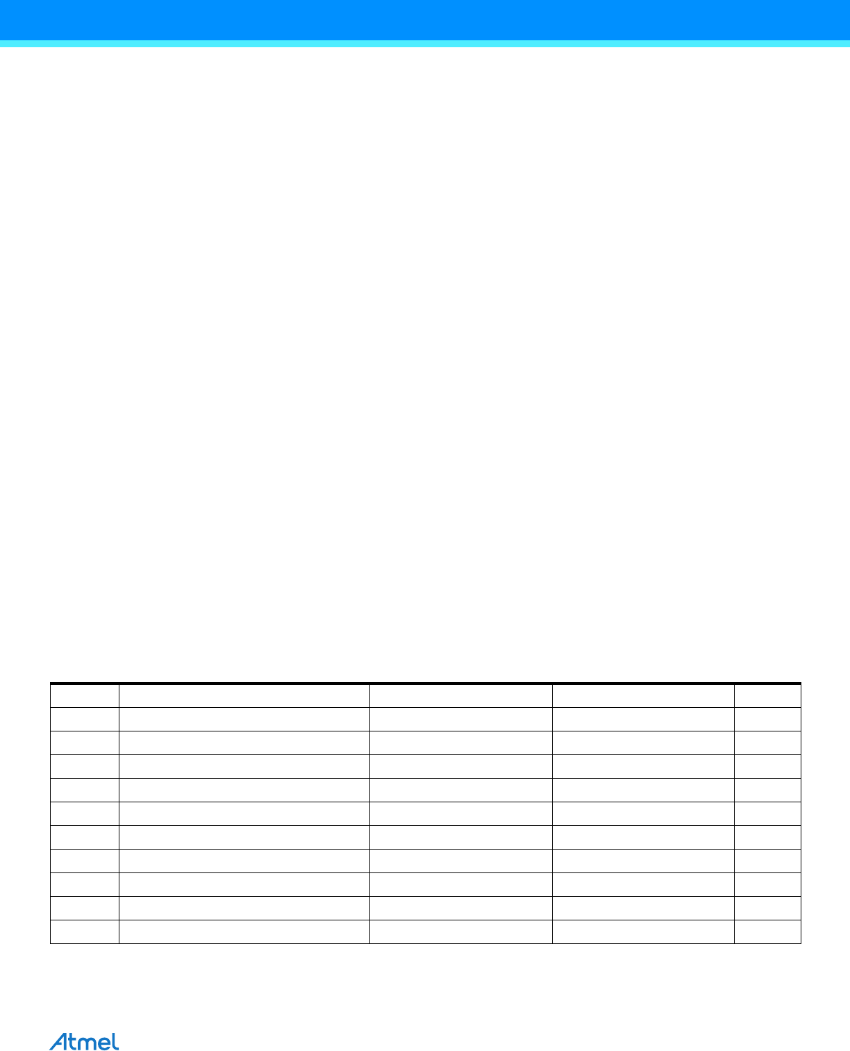
Table 22-1. Register Mapping
Offset Register Register Name Access Reset
0x100 Receive Pointer Register PERIPH
(1)
_RPR Read-write 0x0
0x104 Receive Counter Register PERIPH_RCR Read-write 0x0
0x108 Transmit Pointer Register PERIPH_TPR Read-write 0x0
0x10C Transmit Counter Register PERIPH_TCR Read-write 0x0
0x110 Receive Next Pointer Register PERIPH_RNPR Read-write 0x0
0x114 Receive Next Counter Register PERIPH_RNCR Read-write 0x0
0x118 Transmit Next Pointer Register PERIPH_TNPR Read-write 0x0
0x11C Transmit Next Counter Register PERIPH_TNCR Read-write 0x0
0x120 PDC Transfer Control Register PERIPH_PTCR Write-only -
0x124 PDC Transfer Status Register PERIPH_PTSR Read-only 0x0