
Datasheet
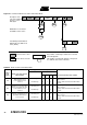
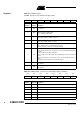
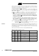
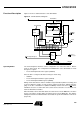
Table Of Contents
- Features
- Description
- Block Diagram
- SFR Mapping
- Pin Configurations
- Oscillators
- Enhanced Features
- Dual Data Pointer Register DPTR
- Expanded RAM (XRAM)
- Reset
- Power Monitor
- Timer 2
- Programmable Counter Array PCA
- Serial I/O Port
- Interrupt System
- Power Management
- Keyboard Interface
- 2-wire Interface (TWI)
- Serial Port Interface (SPI)
- Hardware Watchdog Timer
- ONCE(TM) Mode (ON Chip Emulation)
- Power-off Flag
- EEPROM Data Memory
- Reduced EMI Mode
- Flash Memory
- Electrical Characteristics
- Absolute Maximum Ratings
- DC Parameters
- AC Parameters
- Explanation of the AC Symbols
- External Program Memory Characteristics
- External Program Memory Read Cycle
- External Data Memory Characteristics
- External Data Memory Write Cycle
- External Data Memory Read Cycle
- Serial Port Timing - Shift Register Mode
- Shift Register Timing Waveforms
- External Clock Drive Waveforms
- AC Testing Input/Output Waveforms
- Float Waveforms
- Clock Waveforms
- Ordering Information
- Packaging Information
- Table of Contents

99
AT89C51ID2
4289C–8051–11/05
drive the network. The Master may select each Slave device by software through port
pins (Figure 37). To prevent bus conflicts on the MISO line, only one slave should be
selected at a time by the Master for a transmission.
In a Master configuration, the SS
line can be used in conjunction with the MODF flag in
the SPI Status register (SPSTA) to prevent multiple masters from driving MOSI and
SCK (see Error conditions).
A high level on the SS
pin puts the MISO line of a Slave SPI in a high-impedance state.
The SS
pin could be used as a general-purpose if the following conditions are met:
• The device is configured as a Master and the SSDIS control bit in SPCON is set.
This kind of configuration can be found when only one Master is driving the network
and there is no way that the SS
pin could be pulled low. Therefore, the MODF flag in
the SPSTA will never be set
(1)
.
• The Device is configured as a Slave with CPHA and SSDIS control bits set
(2)
. This
kind of configuration can happen when the system comprises one Master and one
Slave only. Therefore, the device should always be selected and there is no reason
that the Master uses the SS
pin to select the communicating Slave device.
Note: 1. Clearing SSDIS control bit does not clear MODF.
2. Special care should be taken not to set SSDIS control bit when CPHA = ’0’ because
in this mode, the SS is used to start the transmission.
Baud Rate In Master mode, the baud rate can be selected from a baud rate generator which is con-
trolled by three bits in the SPCON register: SPR2, SPR1 and SPR0.The Master clock is
selected from one of seven clock rates resulting from the division of the internal clock by
2, 4, 8, 16, 32, 64 or 128.
Table 77 gives the different clock rates selected by SPR2:SPR1:SPR0.
Table 77. SPI Master Baud Rate Selection
SPR2 SPR1 SPR0 Clock Rate Baud Rate Divisor (BD)
000 F
CLK PERIPH
/2 2
001 F
CLK PERIPH
/4 4
010 F
CLK PERIPH
/8 8
011 F
CLK PERIPH
/16 16
100 F
CLK PERIPH
/32 32
101 F
CLK PERIPH
/64 64
110 F
CLK PERIPH
/128 128
1 1 1 Don’t Use No BRG