
Datasheet
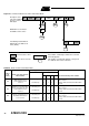
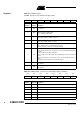
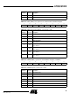
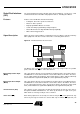
Table Of Contents
- Features
- Description
- Block Diagram
- SFR Mapping
- Pin Configurations
- Oscillators
- Enhanced Features
- Dual Data Pointer Register DPTR
- Expanded RAM (XRAM)
- Reset
- Power Monitor
- Timer 2
- Programmable Counter Array PCA
- Serial I/O Port
- Interrupt System
- Power Management
- Keyboard Interface
- 2-wire Interface (TWI)
- Serial Port Interface (SPI)
- Hardware Watchdog Timer
- ONCE(TM) Mode (ON Chip Emulation)
- Power-off Flag
- EEPROM Data Memory
- Reduced EMI Mode
- Flash Memory
- Electrical Characteristics
- Absolute Maximum Ratings
- DC Parameters
- AC Parameters
- Explanation of the AC Symbols
- External Program Memory Characteristics
- External Program Memory Read Cycle
- External Data Memory Characteristics
- External Data Memory Write Cycle
- External Data Memory Read Cycle
- Serial Port Timing - Shift Register Mode
- Shift Register Timing Waveforms
- External Clock Drive Waveforms
- AC Testing Input/Output Waveforms
- Float Waveforms
- Clock Waveforms
- Ordering Information
- Packaging Information
- Table of Contents
98
AT89C51ID2
4289C–8051–11/05
Serial Port Interface
(SPI)
The Serial Peripheral Interface Module (SPI) allows full-duplex, synchronous, serial
communication between the MCU and peripheral devices, including other MCUs.
Features Features of the SPI Module include the following:
• Full-duplex, three-wire synchronous transfers
• Master or Slave operation
• Eight programmable Master clock rates
• Serial clock with programmable polarity and phase
• Master Mode fault error flag with MCU interrupt capability
• Write collision flag protection
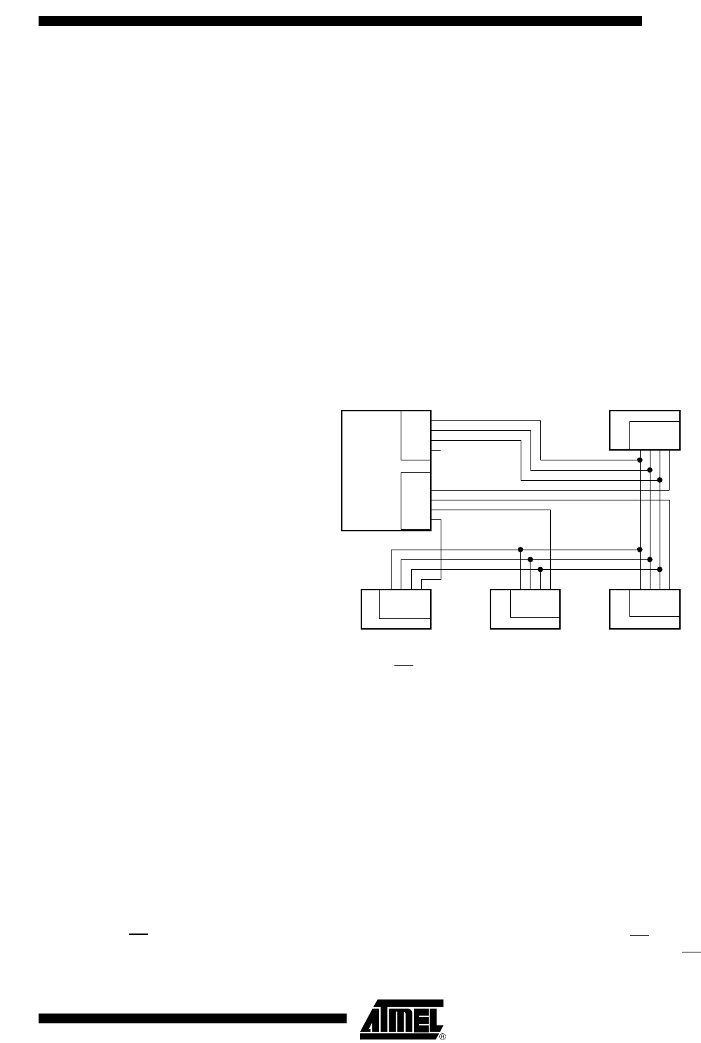
Signal Description Figure 36 shows a typical SPI bus configuration using one Master controller and many
Slave peripherals. The bus is made of three wires connecting all the devices.
Figure 36. SPI Master/Slaves Interconnection
The Master device selects the individual Slave devices by using four pins of a parallel
port to control the four SS
pins of the Slave devices.
Master Output Slave Input
(MOSI)
This 1-bit signal is directly connected between the Master Device and a Slave Device.
The MOSI line is used to transfer data in series from the Master to the Slave. Therefore,
it is an output signal from the Master, and an input signal to a Slave. A Byte (8-bit word)
is transmitted most significant bit (MSB) first, least significant bit (LSB) last.
Master Input Slave Output
(MISO)
This 1-bit signal is directly connected between the Slave Device and a Master Device.
The MISO line is used to transfer data in series from the Slave to the Master. Therefore,
it is an output signal from the Slave, and an input signal to the Master. A Byte (8-bit
word) is transmitted most significant bit (MSB) first, least significant bit (LSB) last.
SPI Serial Clock (SCK) This signal is used to synchronize the data movement both in and out of the devices
through their MOSI and MISO lines. It is driven by the Master for eight clock cycles
which allows to exchange one Byte on the serial lines.
Slave Select (SS
) Each Slave peripheral is selected by one Slave Select pin (SS). This signal must stay
low for any message for a Slave. It is obvious that only one Master (SS
high level) can
Slave 1
MISO
MOSI
SCK
SS
MISO
MOSI
SCK
SS
PORT
0
1
2
3
Slave 3
MISO
MOSI
SCK
SS
Slave 4
MISO
MOSI
SCK
SS
Slave 2
MISO
MOSI
SCK
SS
VDD
Master