
Datasheet
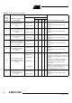
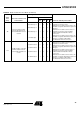
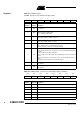
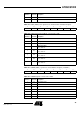
Table Of Contents
- Features
- Description
- Block Diagram
- SFR Mapping
- Pin Configurations
- Oscillators
- Enhanced Features
- Dual Data Pointer Register DPTR
- Expanded RAM (XRAM)
- Reset
- Power Monitor
- Timer 2
- Programmable Counter Array PCA
- Serial I/O Port
- Interrupt System
- Power Management
- Keyboard Interface
- 2-wire Interface (TWI)
- Serial Port Interface (SPI)
- Hardware Watchdog Timer
- ONCE(TM) Mode (ON Chip Emulation)
- Power-off Flag
- EEPROM Data Memory
- Reduced EMI Mode
- Flash Memory
- Electrical Characteristics
- Absolute Maximum Ratings
- DC Parameters
- AC Parameters
- Explanation of the AC Symbols
- External Program Memory Characteristics
- External Program Memory Read Cycle
- External Data Memory Characteristics
- External Data Memory Write Cycle
- External Data Memory Read Cycle
- Serial Port Timing - Shift Register Mode
- Shift Register Timing Waveforms
- External Clock Drive Waveforms
- AC Testing Input/Output Waveforms
- Float Waveforms
- Clock Waveforms
- Ordering Information
- Packaging Information
- Table of Contents
96
AT89C51ID2
4289C–8051–11/05
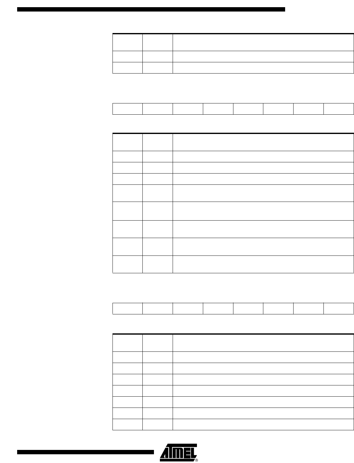
Table 75. SSADR (096h) - Synchronus Serial Address Register (read/write)
Table 76. SSADR Register - Reset value = FEh
1 SD1 Address bit 1 or Data bit 1.
0 SD0 Address bit 0 (R/W) or Data bit 0.
Table 73. SSCS (094h) read - Synchronous Serial Control and Status Register
76543210
SC4SC3SC2SC1SC0 0 0 0
Table 74. SSCS Register: Read Mode - Reset Value = F8h
Bit
Number
Bit
Mnemonic Description
0 0 Always zero
1 0 Always zero
2 0 Always zero
3SC0
Status Code bit 0
See to Table 70.
4SC1
Status Code bit 1
See to Table 70.
5SC2
Status Code bit 2
See to Table 70.
6SC3
Status Code bit 3
See to Table 70.
7SC4
Status Code bit 4
See to Table 70.
76543210
A7 A6 A5 A4 A3 A2 A1 A0
Bit
Number
Bit
Mnemonic Description
7 A7 Slave Address bit 7
6 A6 Slave Address bit 6
5 A5 Slave Address bit 5
4 A4 Slave Address bit 4
3 A3 Slave Address bit 3
2 A2 Slave Address bit 2
1 A1 Slave Address bit 1
Bit
Number
Bit
Mnemonic Description