
Datasheet

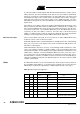
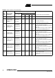
Table Of Contents
- Features
- Description
- Block Diagram
- SFR Mapping
- Pin Configurations
- Oscillators
- Enhanced Features
- Dual Data Pointer Register DPTR
- Expanded RAM (XRAM)
- Reset
- Power Monitor
- Timer 2
- Programmable Counter Array PCA
- Serial I/O Port
- Interrupt System
- Power Management
- Keyboard Interface
- 2-wire Interface (TWI)
- Serial Port Interface (SPI)
- Hardware Watchdog Timer
- ONCE(TM) Mode (ON Chip Emulation)
- Power-off Flag
- EEPROM Data Memory
- Reduced EMI Mode
- Flash Memory
- Electrical Characteristics
- Absolute Maximum Ratings
- DC Parameters
- AC Parameters
- Explanation of the AC Symbols
- External Program Memory Characteristics
- External Program Memory Read Cycle
- External Data Memory Characteristics
- External Data Memory Write Cycle
- External Data Memory Read Cycle
- Serial Port Timing - Shift Register Mode
- Shift Register Timing Waveforms
- External Clock Drive Waveforms
- AC Testing Input/Output Waveforms
- Float Waveforms
- Clock Waveforms
- Ordering Information
- Packaging Information
- Table of Contents
90
AT89C51ID2
4289C–8051–11/05
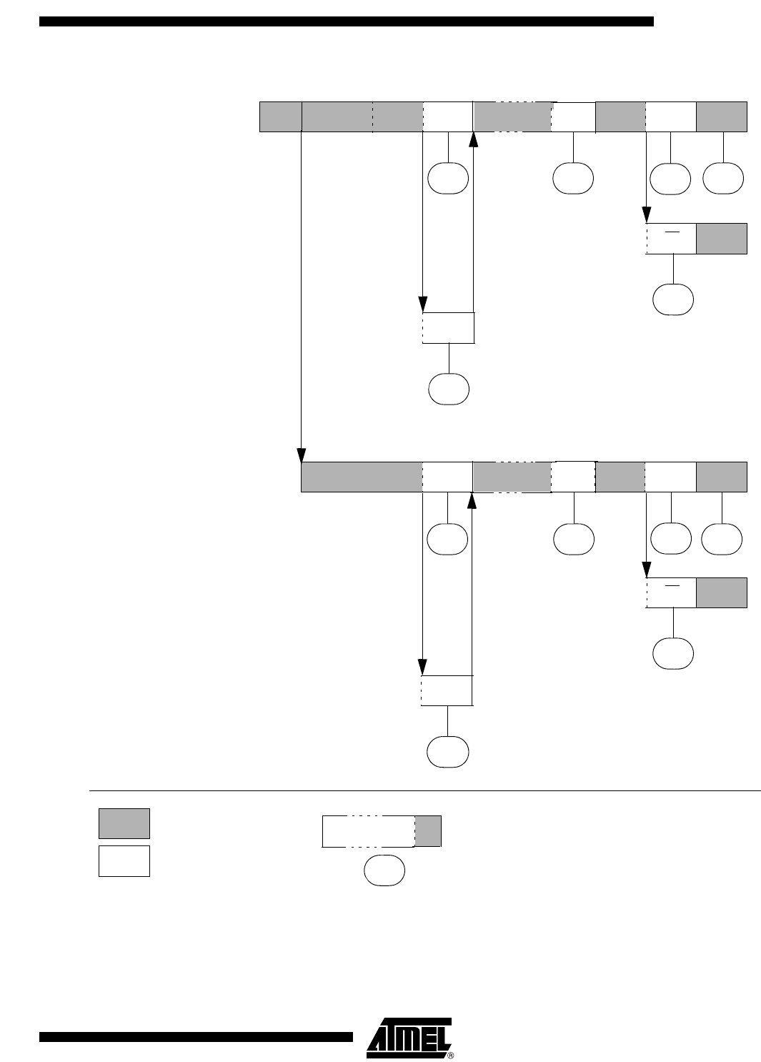
Figure 34. Format and State in the Slave Receiver Mode
SSLAWA
Data
A
Data
P or S
A
P or S
A
General Call A
Data
A
Data
P or S
A
A
60h
68h
80h
80h
A0h
88h
70h 90h
90h
A0h
P or S
A
98h
A
78h
Data A
n
From master to slave
From slave to master
Any number of data bytes and their associated
acknowledge bits
This number (contained in SSCS) corresponds
to a defined state of the 2-wire bus
Reception of the own
slave address and one or
more data bytes. All are
acknowledged.
Last data byte received
is not acknowledged.
Arbitration lost as master
and addressed as slave
Reception of the general call
address and one or more data
bytes.
Last data byte received is
not acknowledged.
Arbitration lost as master and
addressed as slave by general call